Comprehensive Solutions for Material Analysis


Characterise. Understand. Solve.

Advanced materials analysis solutions for your most challenging applications.

Oxford Instruments provides complementary characterisation technologies to help you gain a deeper understanding of your materials from multiple perspectives.
Contact our local team to discuss your research needs and discover the right solutions to accelerate your research.

Talk to our Experts

EDS Detectors for SEM/TEM and FIB

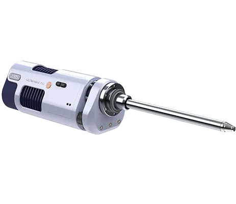
We provide solutions from routine EDS microanalysis that demands high-through-put capabilities to the most advanced NanoAnalysis where performance counts.

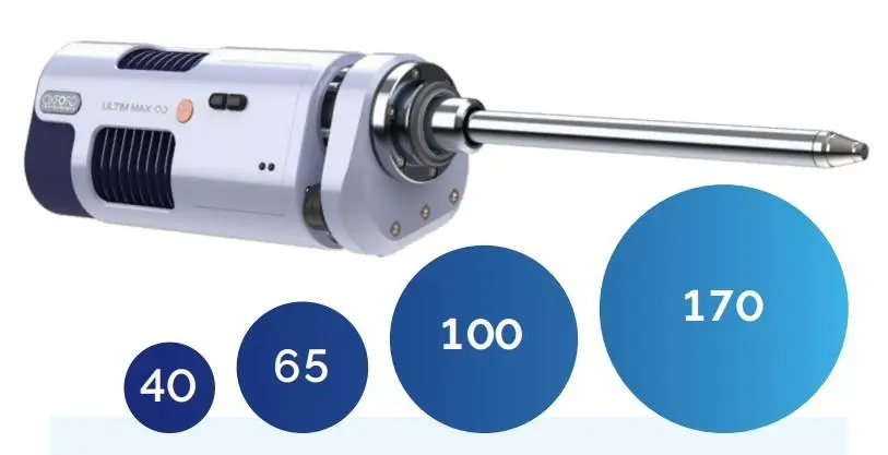
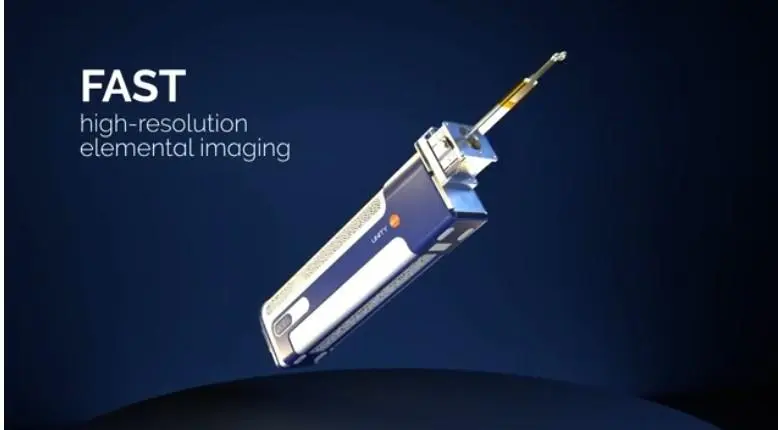
Powered by Ultim Max Infinity SDD detectors that unlock the infinite potential of EDS - including the world's largest area SDD at 170 mm2, and guaranteed Carbon resolution of 46eV or better for all sensor sizes.

  • Offering rapid data collection for live EDS analysis, Xplore guarantees the reliable results required for routine analysis applications
  • We provide turn-key solutions for Gunshot Residue, Mineral Liberation, ThinFilm analysis...and more
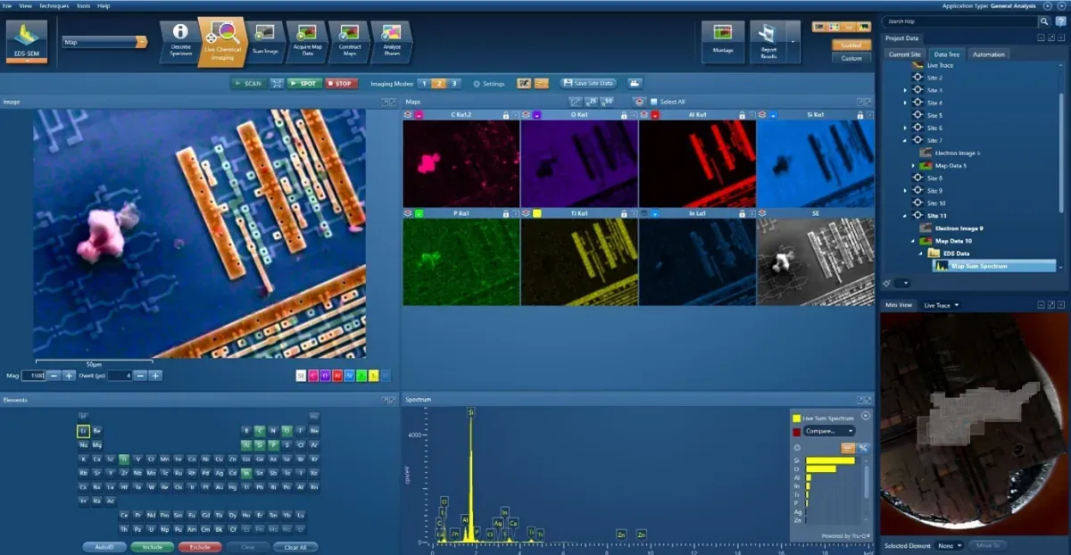
  • Live Chemical Imaging is next phase in the revolutionary AZtecLive Chemical Imaging

Request Pricing

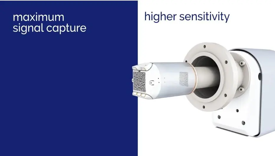
The Ultim Max ∞ (Infinity) SDD detector unlocks the infinite potential of EDS for characterising materials in the SEM. It combines unparalleled accuracy, sensitivity and speed to power AZtecLive software to solve more complex analysis challenges.

Why Infinity

  • The highest sensitivity guaranteed with sensor sizes from 40 mm2 up to 170 mm2 all offering the exact same analytical performance.
  • Resolution guaranteed at CKα of 46 eV or better at all count rates up to 50,000 cps
  • Resolution guaranteed at MnKαP P P of 127 eV or better at all count rates up to 200,000 cps
  • Unique new Tru-Q IQ spectrum processing. Each detector is individually characterised on SEM during manufacturing and optimised for accurate data processing
  • Infinity pulse processing and pile-up correction combine to identify elements and display artefact-free element distribution
Download Brochure Learn more

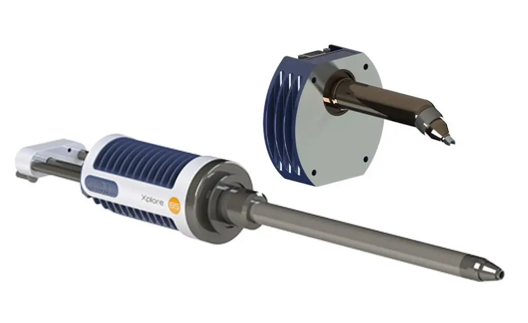
Xplore is a high throughput compact EDS detector designed for routine microanalysis in the SEM. It’s innovative design means that it has the quality and accuracy you expect from the class leading Ultim Max Infinity large area detectors, but in a much smaller package.

Reduction in cost and complexity but not at the expense of accuracy, reliability or quality.

Key Features

  • Sensor Sizes: Available in 15 mm2, 30 mm2 and 65 mm2 sensor sizes.
  • Speed: Mapping can be carried out at count rates >1,000,000 cps.
  • Guaranteed Resolution: Mn Kα res guaranteed to be <129 eV at 100 Kcps for all sensor sizes.
  • Analysis at realistic count rates: Quantitative analysis at count rates > 100 Kcps.
  • Detection range: Detection from beryllium (Be) to californium (Cf) - 30mm2 and 65mm2. Detection from boron (B) to californium (Cf) – 15mm2
Download Brochure Learn more

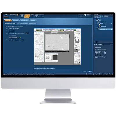
AZtecLive is the software that when powered by Ultim Max Infinity brings the infinite potential of EDS to life. See how live chemical imaging is a new approach to sample investigation and understand our workflows for qualitative and quantitative analysis as well as X-ray mapping and linescanning. 

Discover the tools that can help you use EDS to solve your characterisation challenges in the SEM.

Learn more

Learn what is now possible with Infinity detectors from Oxford Instruments

  • What is new and different about Infinity EDS detectors
  • How Tru-Q IQ individual detector optimised spectrum processing increases accuracy and sensitivity
  • How these new technologies allow us to characterise smaller and more complex nano-structures
  • How EDS can map faster, more accurately and is starting to rival the sensitivity of WDS for some applications

CMOS EBSD Detectors 

The best all-round EBSD detectors combined with superior analytical software

Our CMOS range of detectors , including the market-leading Symmetry S3, the C-Nano+ and the C-Swift+, all deliver exceptional performance for every type of EBSD analysis. Benefiting from a unique lens-free fibre optic design, our CMOS detectors combine unparalleled sensitivity with excellent analysis speeds, ensuring optimum data quality from any sample.

Request Pricing

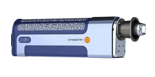
The Symmetry S3 is the only genuine all-in-one EBSD detector on the market, and is based on the revolutionary Symmetry detector, the world’s first EBSD detector to utilise advanced CMOS technology. 

  • Guaranteed indexing speeds in excess of 5700 pps at 156 x 128 pixel EBSD pattern resolution
  • 1244 x 1024 pixel resolution – ideal for high angular resolution (HR) EBSD
  • Unique fibre-optic coupling with sub-pixel distortion
  • Extreme sensitivity, benefiting all types of analysis
  • Software controlled detector tilting
  • Highest sensitivity > 1000 pps / nA
  • Sub-pixel distortion, ensuring an angular precision below 0.05°

Learn more

The C+ series EBSD detectors, the C-Nano+ and the C- Swift+, are 2nd generation entry-level detectors designed for every type of EBSD application.

The C-Nano+ delivers a top acquisition speed exceeding 600 pps with exceptional 311 x 256 pixel resolution patterns: this makes it about 5-6 times faster than comparable CCD-based detectors, , using patterns with at least 4 times as many pixels.

  • Full 1244 x 1024 pixel resolution patterns – ideal for high resolution EBSD
  • Class-leading acquisition speed of > 600 pps
  • Fibre optics delivering extreme sensitivity for low energy and low current analyses
  • Distortion free images
Learn more

The C-Swift+ uses a customised CMOS sensor coupled with fibre optics, to deliver both speed and sensitivity, ensuring high quality results on even the most challenging materials.

  • Guaranteed indexing speeds of > 2000 pps
  • 622 x 512 pixel EBSPs at 250 pps
  • Fibre optics delivering extreme sensitivity for low energy and low current analyses
  • Distortion free images
Download Brochure Learn more

AZtecHKL is a flexible yet intuitive EBSD data acquisition software platform, designed for ease of use and to deliver consistently high-quality results. Based around a series of dedicated navigators and fully integrated with EDS, AZtecHKL makes any type of EBSD or transmission Kikuchi diffraction (TKD) data acquisition a routine task.

  • Tailored Workflow that brings Oxford Instruments’ EBSD expertise to optimise system configuration for recurring measurement requirements.
  • EBSD Shadow Masking reduces the impact of shadows caused by rough or complex sample geometries
  • Batch Export streamlines post-acquisition data handling and transfer into established analysis, archiving, and reporting workflows.
  • HTML Project Report provides a consistent record of measurement setup, acquisition, and analysis to support clear communication of findings.
  • Tru-I Indexing Engine ensures that users collect the best quality patterns and can solve them accurately, reliably and automatically.
Learn more

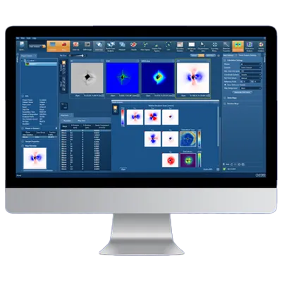
AZtecCrystal is a future-proof, innovative EBSD data processing software package that combines a modern interface with a host of high-end functionality. Constantly developing, AZtecCrystal now includes unique tools such as dislocation analysis & parent grain reconstruction, with MapSweeper enabling advanced dataset reanalysis using pattern matching techniques.

Download Brochure Learn more

Unity BEX Imaging Detector

Unity's innovative design incorporates both backscattered electron and X-ray sensors within a single package, strategically positioned directly beneath the pole piece to maximise signal collection while eliminating shadowing effects from unpolished samp les.

Using the latest advancements in Energy Dispersive Spectroscopy (EDS) technology, including ultra-fast electronics and advanced spectrum processing algorithms, the Unity BEX/EDS system sets a new standard for elemental analysis in SEM. With increased sensitivity and speeds up to 100 times faster than conventional systems, Unity enables the analysis of sensitive samples, rough surfaces, and trace elements (>0.1 wt%), all under standard SEM imaging conditions.

Request Pricing

Download Brochure Learn more

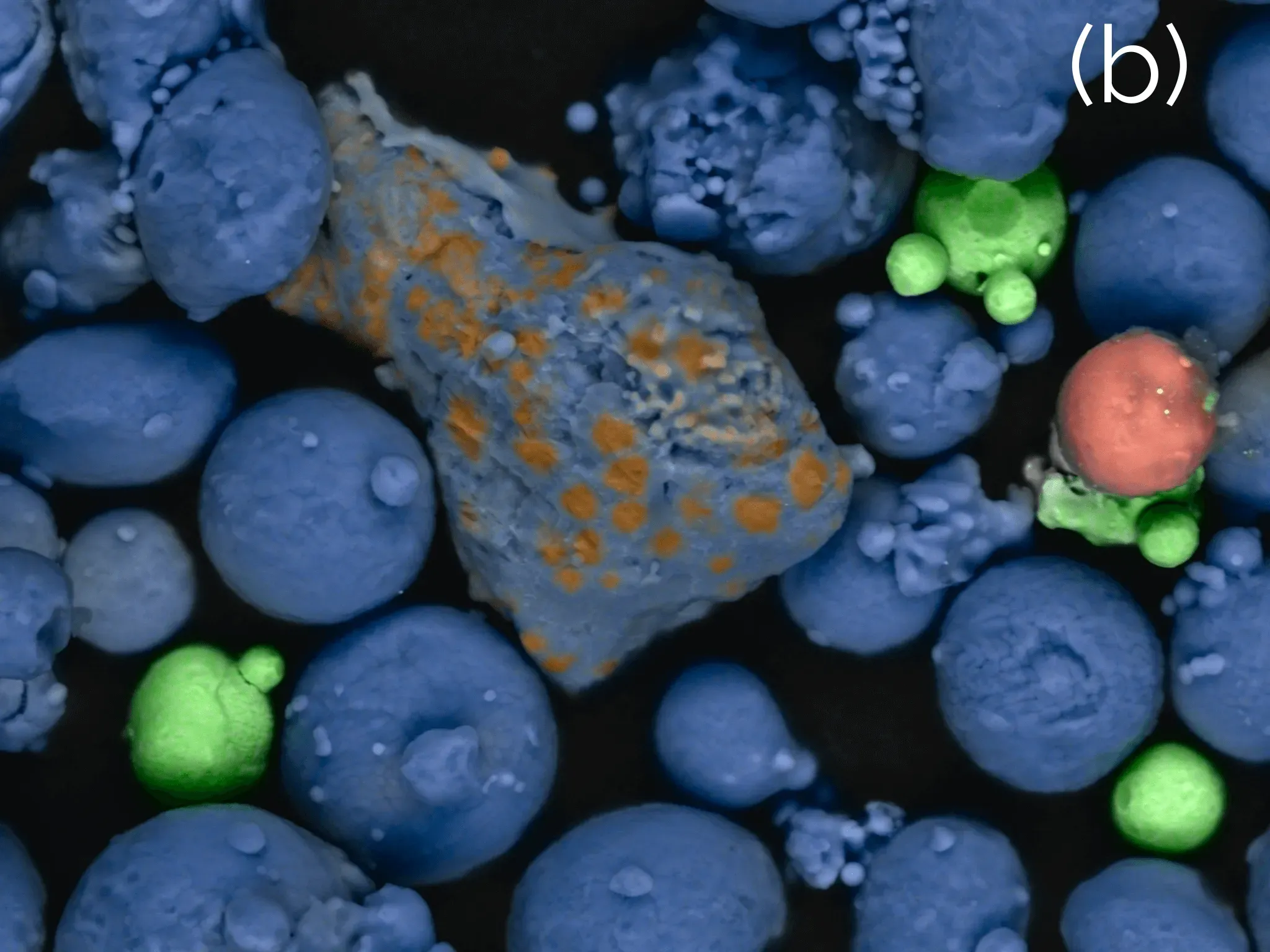
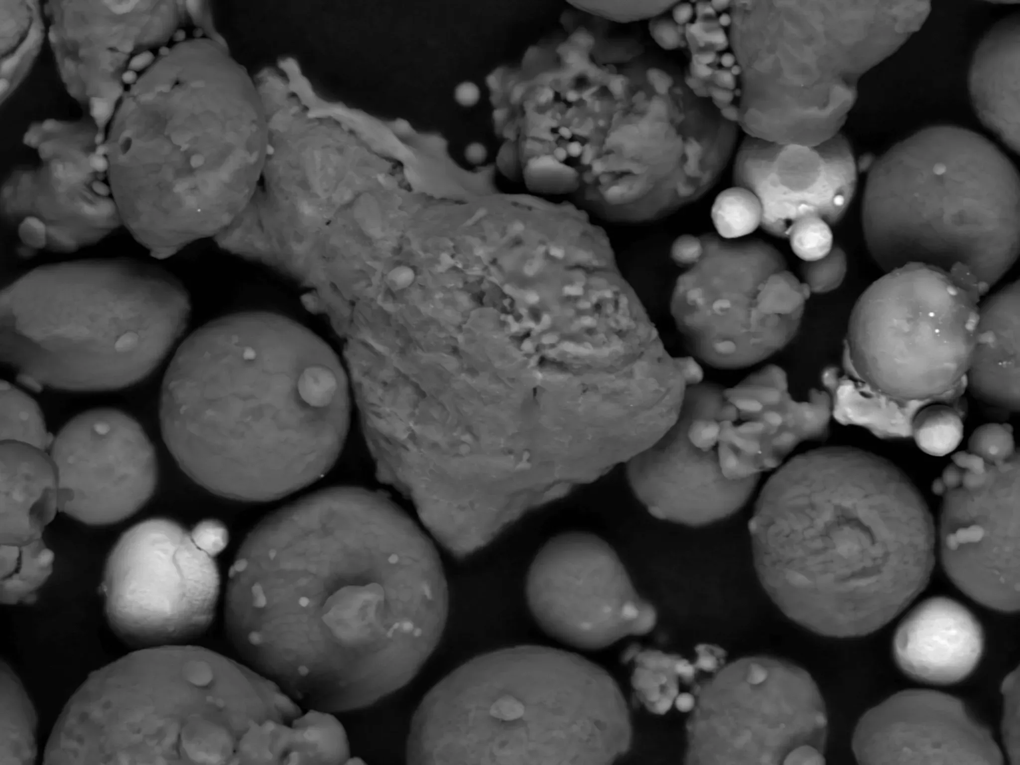
BEX is a pioneering analytical technique for SEM. BEX combines Backscattered Electron and X-ray (BEX) imaging in a single technique, simultaneously. In an industry breakthrough, the best of both techniques are integrated to accelerate your time to discovery.

Learn more
BEX coloured electron image
Backscattered electron image

How the BEX technique is changing the way we use SEM

Discover more about the BEX imaging technique and see how the Unity detector will revolutionise analysis in scanning electron microscopy using a variety of sample types to show the power of this new technology in action

You will learn:

  • Basics of the BEX technique and the Unity detector
  • How BEX is used to solve real issues, using examples from Battery, Geology, Alloys and Electronics
  • How BEX can be used in extreme conditions like variable pressure mode & high magnifications

Confocal Raman Imaging Microscopes

Oxford Instruments' confocal Raman imaging microscopes deliver advanced chemical characterization with industry-leading speed, sensitivity and resolution – simultaneously.

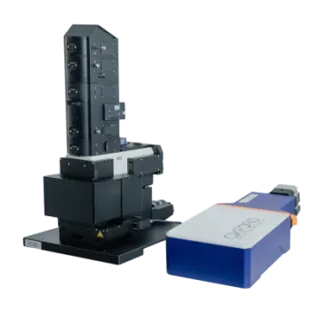
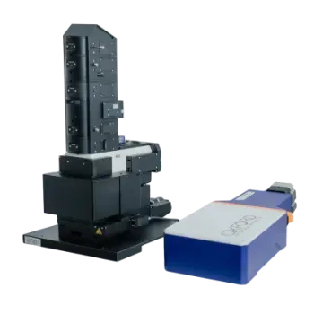
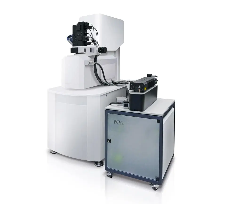
The witec360 microscopes include variations for every budget environment and sample type. Through a modular hardware and software architecture, the systems can be configured for individual requirements and reconfigured as experiments evolve. Excitation wavelengths from the UV through VIS to the NIR are available and their fiber-based beam delivery provides a flexible laboratory footprint.

Request Pricing

The witec360 sets the highest standards for performance in confocal Raman imaging. Every component is optimised for maximum transmission efficiency and consistency, enabling accurate results within seconds. This accelerates your imaging workflows and facilitates even the most challenging applications.

Why witec360

  • High performance, research grade Raman imaging system
  • Correlative Raman analysis with PL, AFM, SHG, TCSPC, profilometry & SEM
  • Modular, customisable & future-ready setup
  • Broadband spectral range from UV excitation to NIR with class leading resolution
  • Extensive automation options and intuitive multi-user access
Download Brochure Learn more

World's first fully integrated Raman Imaging and Scanning Electron Microscopes

RISE Microscopy is a novel correlative microscopy technique that combines SEM and confocal Raman Imaging. Through RISE Microscopy ultra-structural surface properties can be linked to molecular compound information.

  • Quick and convenient switching between Raman and SEM measurement
  • Automated sample transfer from one measuring position to the other
  • Integrated software interface for user-friendly measurement control
  • Correlation of the measurement results and image overlay
  • No compromise in SEM and Raman imaging capabilities
Download Brochure Learn more

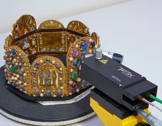
alphaCART is Oxford Instruments' mobile, confocal Raman system for all applications that require bringing the lab to the sample.

The system's high confocality and signal sensitivity also allow measurements through protective glass and windows, which enables studies of gases or chemical processes inside reaction chambers and other enclosures. Researchers working in the arts and archaeology, geo- or materials science will especially benefit from this versatile and powerful analytical tool.

Benefits

  • Oversized samples that don’t fit under a microscope
  • Fragile or precious objects that can’t be moved to a lab
  • Samples that exhibit fluorescence, as background is minimized
  • Gases and liquids inside glass containers, as even weak signals can be detected
  • Samples at high temperature, as background from black body radiation is effectively minimized
  • Samples at high temperature, as background from black body radiation is effectively minimized
Download Brochure Learn more

Atomic Force Microscopy

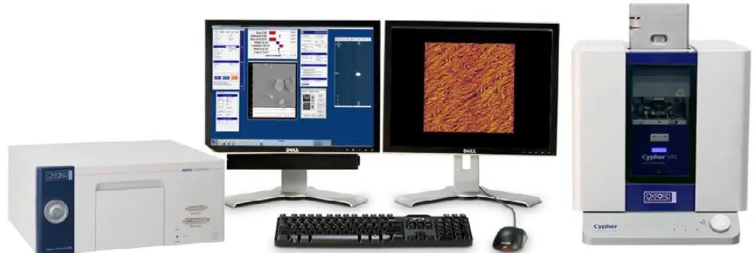
Oxford Instruments Asylum Research AFMs are widely used by both academic and industrial researchers for characterizing samples from diverse fields spanning material science, polymers, thin films, energy research, and biophysics.

In addition to routine imaging of sample topography and roughness, Asylum Research AFMs also offer unmatched resolution and quantitative measurement capability for nanoelectrical, nanomechanical, and electromechanical characterization.

Recent advances have made these measurements far simpler and more automated for increased consistency and productivity. Its Cypher, MFP-3D, Jupiter, and Vero AFM product lines span a wide range of performance, versatility, and budgets.

Request Pricing

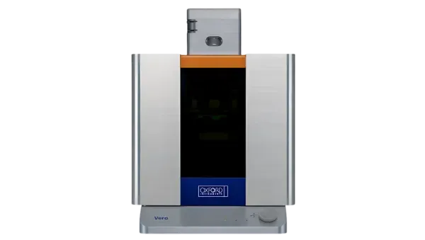
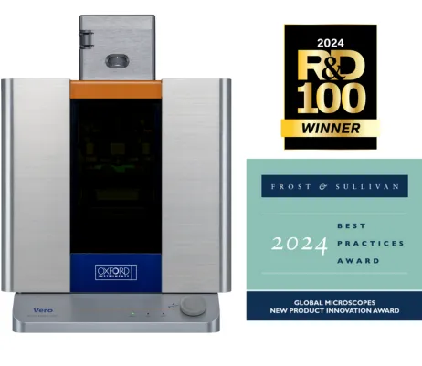
Meet our next-generation AFMs that precisely and accurately measures true tip displacement using Quadrature Phase Differential Interferometry (QPDI). Built on the unrivaled stability and performance of the Cypher AFM family, this unique patented QPDI innovation enables Vero AFMs to provide results with higher accuracy, precision, and repeatability.

Quadrature Phase Differential Interferometry:

  • Measures true tip displacement
  • Improves measurement sensitivity
  • Avoids crosstalk between vertical and in-plane forces
  • Is precisely calibrated by the wavelength of light
Download Brochure Learn more

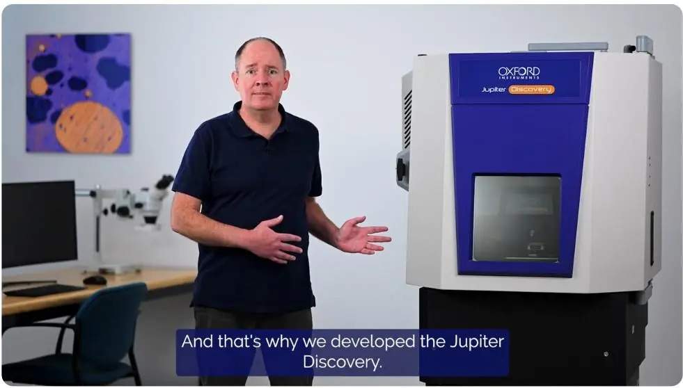
Large-Sample AFM with Superior Resolution, Speed, Ease of Use, and Flexibility – capable for samples up to 210 mm diameter.

  • Pre-mounted probes: Users handle pre-mounted probes with their fingers instead of tweezers, eliminating a common frustration.
  • Guided workflow: A simple interface walks users through setup. Once the probe and sample are placed, all steps are controlled via software, reducing complexity and risk of damage.
  • Side-view camera: This unique feature makes it easy to gauge the distance between the probe and sample, enabling users to confidently engage the AFM and start imaging.
  • FFM-Topography with AutoPilot: This exclusive imaging mode makes imaging as simple as selecting a scan area and clicking Start, with algorithms automatically optimizing scan parameters.
Download Brochure Learn more

Proven AFMs engineered for exceptional resolution, speed, and versatility

The Cypher Family delivers industry-leading AFM performance built on an ultra‑stable, low‑noise platform - enabling fast & high‑resolution imaging and broad research versatility across materials science and life science disciplines.

  • Gold standard for 2D materials research
  • Consistently achieve higher resolution than other AFMs
  • Fast scanning with results in seconds instead of minutes
  • Motorized laser and photodiode positioning simplifies setup and operation
  • Small footprint in the lab, huge potential to grow in capability
Download Brochures Learn more

Nanoindentation

Accuracy, Speed, Operando Testing

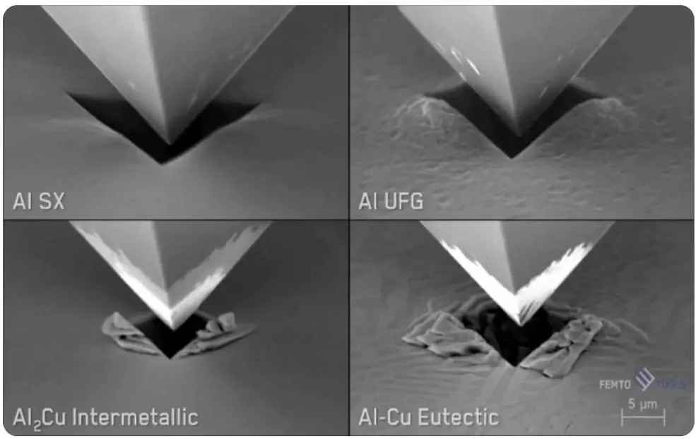
FemtoTools, now proudly part of Oxford Instruments, continues to lead in ultra-precise mechanical testing solutions. With a legacy of Swiss engineering excellence, our cutting-edge technologies empower researchers, engineers, and manufacturers to measure the smallest forces with unmatched accuracy. As part of a global scientific instrumentation leader, we’re bringing our innovations to more markets and accelerating the future of micro- and nanomechanical testing.

Request Pricing

Ultra-fast nanoindentation in operando conditions

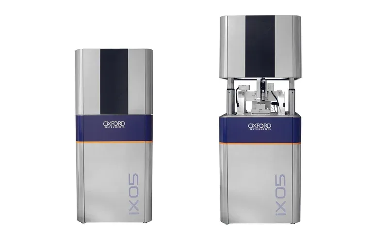
The iX05 nanoindenter is a standalone MEMS-based nanoindenter optimized for material property analysis in a wide range of operando conditions such as at high-temperature, at low-temperature, at high strain rates.

Why iX05?

Operando Nanoindentation

  • High-temperature nanoindentation with active tip heating for isothermal testing at temperatures up to +800°C
  • Cryogenic nanoindentation at temperatures down to -150°C

Ultra-Fast Nanoindentation

  • Ultra-fast nanoindentation at speeds up to 30 indentations per second
  • Unmatched performance at ultrahigh speeds: FemtoTools MEMS force sensor (resonance at up to 100 kHz) combined with ultra-fast electronics (2 MHz sampling rate, 500 kHz feedback frequency)

Ultra-High Resolution 

Ultra-high resolution nanoindentation with unmatched repeatability to detect even the smallest variations in hardness and modulus

Download Brochure Learn more

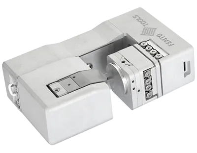
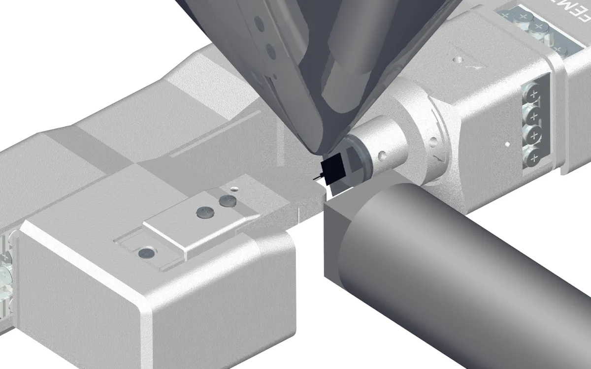
In-situ FIB/SEM nanoindenter for compression, tensile and fracture testing of micro- and nanoscale samples with simultaneous high resolution imaging of the tested sample using SEM.

Why NMT04?

  • Unmatched Dynamic Range: Micro-Electro-Mechanical System (MEMS)-based force sensors have an unmatched dynamic range of up to 100 kHz, thanks to their exceptionally small mobile mass and high stiffness. Moreover, the fine fabrication tolerances of MEMS achieve the lowest possible noise floor, reaching down to 500 pN.
  • True Displacement Control: Displacement-controlled nanoindentation is essential for measuring and comparing mechanical properties at consistent indentation depths, ensuring the probing of equivalent material volumes.
  • Open Measurement Frame: The NMT04 is specially-designed to work seamlessly with Electron Backscatter Diffraction (EBSD) or Scanning Transmission Electron Microscopy (STEM) detectors inside the SEM. Its open measurement frame enables simultaneous observation and analysis of the evolution of the microstructure of the sample during mechanical testing.
Download Brochure Learn more

Standalone nanoindenter for high resolution high-speed measurement of local mechanical properties of materials in air, liquid or inert gas environment

Why iO4?

  • Micro-Electro-Mechanical System (MEMS)-based force sensors have an unmatched dynamic range of up to 100 kHz, thanks to their exceptionally small mobile mass and high stiffness. Moreover, the fine fabrication tolerances of MEMS achieve the lowest possible noise floor, reaching down to 500 pN.
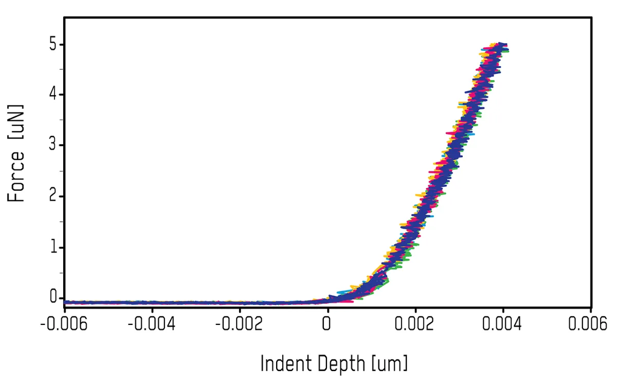
  • A key quality metric of a nanoindenter is its ability to accurately measure indentation depth. This is limited by the noise floor (resolution) of the displacement sensor. With an unmatched noise floor of <50 pm, the i04 Femto-Indenter achieves excellent results even at the most shallow depths, as shown here with repeatable indentation curves to only 5 nm on quartz glass.
  • Displacement-controlled nanoindentation is essential for measuring and comparing mechanical properties at consistent indentation depths, ensuring the probing of equivalent material volumes.
Download Brochure Learn more