Modern products increasingly utilize engineered surface functionalities to achieve superior performance, such as hydrophobicity for self-cleaning window glass. These properties result from tailored surface chemistry to change adhesion and surface free energy. Nanoindentation is an attractive technique for such measurements. For a nanoindentation system to perform this application, three factors are important to remember: force resolution, displacement control, and environmental controls. Nanoindentation measurements are successfully demonstrated on a variety of engineered surfaces, even at sub-micronewton force levels. Adhesion measurements on silicon show ideal force-displacement relationships with measured SFE values in good agreement with literature values.
Introduction
Engineered surface properties play a key role in many modern products. This includes not only the control of surface topography and roughness but also the surface chemistry. This allows the engineering of adhesion and friction behavior to reduce wear or to achieve properties such as hydro-, oleo-, or ice-phobicity or -philicity. These have applications ranging from self-cleaning glass for architecture and repelling fingerprints from smartphone screens to anti-icing surfaces for aerospace. To improve these engineered surfaces, accurate and rapid measurement of adhesion and surface free energy (SFE) is essential.
Traditionally, surface free energy and wettability is measured using contact angle measurement (CAM). The contact angle is geometrically defined as the angle formed by a liquid drop at the three-phase boundary where a liquid, gas, and solid intersect. Standard CAM measurements require drops of several different liquids on a relatively large, flat surface and determining the contact angles for each liquid [1]. This can be difficult for small areas of nano-patterned surfaces or curved surfaces. This makes surface free energy measurements using a nanoindenter to be an attractive alternative [2], due to their ease of use, non-destructive, and local measurement capabilities.
In this application note, nanoindentation measurement of adhesion and surface free energy is demonstrated on several different surfaces. Details of the approach are described, particularly the system concerns, and the ability of nanoindentation to measure adhesion is discussed and demonstrated.
Experimental Considerations
For a system to perform this application, three factors are important to remember: force resolution, displacement control, and environmental controls. For clear resolution of the forces as a function of distance from the surface, displacement control is essential. As adhesive forces can be very small, having a sensor with the appropriate force resolution is critical to resolve the phenomenon, and environmental controls are important to prevent humidity effects on the data.
Low Force Measurement
Adhesive forces can arise from long range Van de Waals forces and surface free energy effects. These can be exceedingly small and require high force resolution for precision measurements. Depending on the indenter material and radius, and surface properties, adhesive forces for a material can vary over several orders of magnitude. Oxford Instruments nanoindentation systems offer a range of sensors with ranges from millinewton down to sub-nanonewton forces - Table 1.
Table 1. FT-S Microforce sensing probes specifications in the lower force ranges.
|
Sensor
|
Force Range
|
Resolution
@ 10 Hz
|
|
FT-S200
|
±200 µN
|
0.0005 µN
|
|
FT-S2,000
|
±2,000 µN
|
0.005 µN
|
|
FT-S20,000
|
±20,000 µN
|
0.05 µN
|
|
FT-S200,000
|
±200,000 µN
|
0.5 µN
|
Depending on the size of the region of interest and surface roughness, additional scaling effects can also be achieved by varying the indenter radius to increase or decrease the relative magnitude of the adhesive forces. A larger tip radius results in greater pull-off forces, thereby improving measurement sensitivity, which is especially beneficial for hydrophobic materials.
Displacement Control
As in many other applications, displacement control is preferred for adhesive measurements to prevent dynamic events from obscuring displace-force relationships. In an ideal adhesive contact measurement between a flat surface and a round indenter (Figure 1),
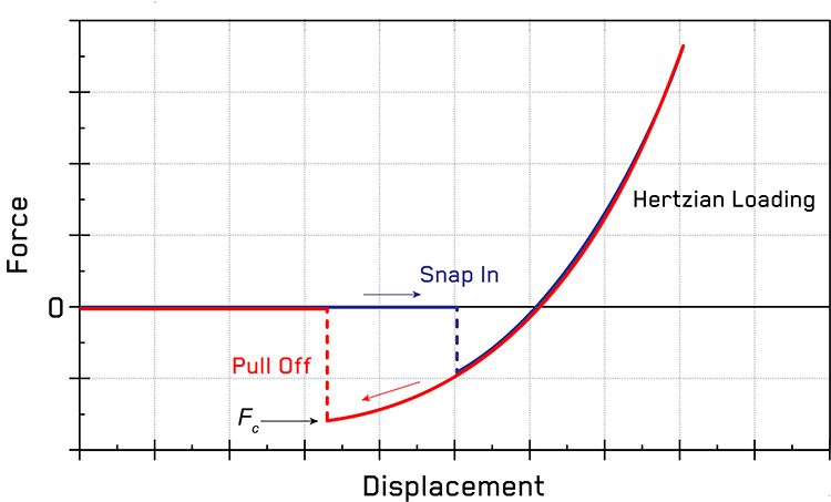
Figure 1. Ideal force-displacement curves for adhesive contacts due to surface free energy, after [2].
Environmental Control
Relative humidity has a strong influence on wettability and adhesion measurements, even using CAM [3] techniques. To control for this, adhesion measurements need to be performed at well-defined levels of relative humidity. This can be done either using a closed system with an integrated environmental control, through gas purging using dry nitrogen, or using desiccants to remove moisture from the chamber.
Experimental Procedures
Silicon samples were provided as part of a VAMAS international interlaboratory study, which was organized by the European Horizon 2020 project Oyster (Open characterization and modelling environment to drive innovation in advanced nano-architectured and bio-inspired hard/soft interfaces). Surface treatments to the silicon wafers were performed using atmospheric plasma treatment to give superhydrophobic, hydrophobic, hydrophilic, and super hydrophilic surfaces. These were characterized by one of the interlaboratory study partners using confocal optical profilometry (Figure 2).
Mechanical microscopy was performed using an NMT04 In-Situ SEM Nanoindenter with a FT-S2000 sensor fitted with a 105 µm radius sapphire sphere. Tests were performed in the chamber of a Zeiss EVO 25 SEM, which was evacuated then purged with dry nitrogen gas to achieve relative humidity levels of < 5%. This was monitored using a Sensirion SHT4x humidity sensor.
As only the initial contact is of interest for this type of measurement, the approach parameters are important to manage so that plastic deformation of the surface can be prevented. For this purpose, very low trigger forces (0.1 µN) were used to define the contact. The approach velocity was set to 10 nm/s with a target maximum depth of 20 nm. The test profile was defined by the project to be 5 s loading, 3 s dwell time, and 5 s unloading.
Results
The measured force-displacement curves and surface topologies measured from the bare silicon, hydrophilic and superhydrophilic surfaces are shown in Figure 2. Pronounced differences in the surface roughness and topology of the various surface treatments can be immediately observed, especially in the relative magnitude of the topologies highlighted by the differences in the respective scale bars. The bare silicon surface is extremely smooth with roughness values on the order of 10 nm, while the other coatings possess features in the 100s or 1000s of nm.
The results from the bare silicon indicate behavior nearly identical to ideal predictions, Figure 1, with nearly vertical pull-off and snap-in events followed by Hertzian contact. This appears nearly linear given the relative scale of the 105 µm radius indenter and displacements in the 10s of nm. Adhesion forces are relatively large in the 10s of µNs.
The hydrophilic and superhydrophilic surfaces show very different behavior from the bare silicon. The force-displacement curve shows some plastic deformation, likely of the asperities, and the snap-in and pull-off forces shown more complicated behavior, rather than sharp snap-in or pull-off features. These adhesion forces are orders of magnitude smaller than the flat, bare silicon, which likely indicates contact with asperities with this large indenter radius. A small force relaxation is observed at the maximum displacement during the dwell period in both cases.
In the case of the superhydrophilic surface, long range Van der Waals forces can also be seen as the small negative deviation in the force as it approaches the surfaces during the last ~150 nm of displacement. This is clearly due to an attractive force, not measurement drift, as it is identical on both approach and retraction.
These force-displacement curves highlight the nanonewton resolution of the FT-S2,000 sensors. This allows not only the snap-in and pull-off forces to be clearly observed but also the displacement control of the measurement allows the complex force-displacement relationships to be characterized without any mechanical instabilities. This allows work of adhesion energies to be calculated in a straightforward manner.
![Ideal force-displacement curves for adhesive contacts due to surface free energy, after [2].](https://www.oxinst.com/learning/uploads/inline-images/ni-an5-fig1-750-20250527152152.png) Figure 2. Force-displacement curves for the bare silicon, hydrophilic, and super hydrophilic surfaces along with their corresponding surface topologies from confocal profilometry.
Figure 2. Force-displacement curves for the bare silicon, hydrophilic, and super hydrophilic surfaces along with their corresponding surface topologies from confocal profilometry.
Discussion
Analysis of adhesion behavior via nanoindentation is still under active development [2]. However, there are several models which can be applied to determine surface free energies from adhesive forces. The measured pull-off forces can be used to calculate the material’s SFE by using either the Johnson–Kendall–Roberts (JKR) or Derjaguin–Muller–Toporov (DMT) models. JKR more accurately describes interactions between compliant bodies with larger elastic deflections, and DMT is more accurate in describing interactions between stiff bodies with smaller contact radii. A survey of the various adhesion regimes and transitions in behavior between these two popular models can be found in the work of D. Maugis [4].
Thus, the JKR and DMT models represent the upper and lower bounds of contact–adhesion models for determining SFE values. These are represented by two similar equations. The JKR model is represented by
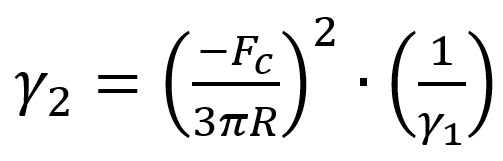 and the DMT model is represented by
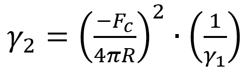 where the SFE of the sample is a function of the pull-off force, Fc , the tip radius, R, and the surface energy of the indenter material, . Both models assume the surface to be flat, so we will only consider the bare silicon sample in this analysis.
From these two equations, it’s clear that the SFE of the indenter’s material, , must be well known to accurately determine a surface’s SFE, . Literature values for the SFE of sapphire range between 43.7 mJ/m2 [5] and 52.95 mJ/m2 [6], and this is expected to vary with the crystallographic plane. As the indenter employed in this case is a sphere with unknown orientation, for these measurements the lower value of = 43.7 mJ/m2 was assumed. For reference, if a diamond indenter was employed instead, would be 43 mJ/m2 [7].
Using these values, the measured value of SFE for the bare silicon from the JKR model was 82.00 ± 0.22 mJ/m2 and 46.12 ± 0.12 mJ/m2 by the DMT model. The DMT model is likely more accurate in this case, as both silicon and sapphire are very stiff. This is in good agreement with literature values for the SFE of Silicon, which vary significantly: 42 mJ/m2 [8], 58.9 [7], and 28.4-60.1 [9]. Our value from the DMT model is quite consistent with the average of these literature values, but an intermediate value between DMT and JKR models may be more accurate due to the large contact radius employed for these measurements.
Conclusion
In this application note, nanoindentation was employed to investigate the contact adhesion of several silicon surfaces. Nanoindentation is an attractive technique for such measurements, as it allows local, rapid measurements on complex surfaces which may be difficult to investigate using conventional contact angle measurements using liquid drops. By using a system with a force resolution in the nanonewton regime with displacement control in a humidity-controlled environment, force-displacement curves were acquired on bare, hydrophilic and superhydrophilic surfaces. Results on bare silicon displayed force-displacement relationships that closely parallel theoretical expectations, and SFE values determined from these forces are in good agreement with literature values for silicon. This successfully demonstrates the application of nanoindentation for surface free energy measurements, which offers an attractive alternative method for the development of novel functionalized surfaces.
Acknowledgements
This work was performed in collaboration with the H2020 Oyster project, which supplied the samples for testing as part of a VAMAS interlaboratory study. This project has received funding from the European Union’s Horizon research and innovation programme under grant agreement number 760827.
References
- F. Etzler, Rev. Adhesion and Adhesives, 1 (2013) 3.
- E. Rossi, P.S. Phani, R. Guillemet, J. Cholet, D. Jussey, W. Oliver, M. Sebastiani, Journal of Materials Research, 36 (2021) 2357-2370.
- Holysz, M. Miroslaw, K. Terpilowski, A. Szczes, in: Annales Universitatis Mariae Curie-Sklodowska, Maria Curie-Skłodowska University, 2008, pp. 223.
- D. Maugis, Journal of Colloid and Interface Science, 150 (1992) 243-269.
- L. Holysz, E. Chibowski, Langmuir, 8 (1992) 717-721.
- E. Dobrovinskaya, L. Lytvynov, V. Pishchik, Properties of Sapphire, in, 1970, pp. 55-176.
- L. Mazzola, M. M. Sebastiani, E. E. Bemporad, F. F. Carassiti, Journal of Adhesion Science and Technology, 26 (2012) 131-150.
- L. Hołysz, M. Mirosław, K. Terpilowski, A. Szcześ, Annales Umcs, Chemistry, 63 (2008) 223-239.
- F. Hejda, P. Solar, J. Kousal, in: WDS, 2010, pp. 25-30.

