Tags: Multi-scale mechanical microscopy, Mechanical Microscopy, Correlative Mechanical Microscopy
Mechanical microscopy allows the imaging of mechanical property variations at multiple length scales. Nanoindentation mapping is usually performed at the microstructural length scale, but many manufacturing processes create property variations on larger scales, e.g. case hardening, nitriding, or designed variations through additive manufacturing. In this series of application notes, we demonstrate how mechanical microscopy can be performed at multiple length scales to connect large-scale variations in mechanical properties to their mechanical properties on a microstructural length scale. This demonstrates the wide range of measurements possible with Oxford Instruments Nanoindentation systems. In this third note, we demonstrate the ability of multi-scale nanoindentation mapping to segment and extract phase-level, constituent properties from complex alloys with phases of varying length scale.
Introduction
Mechanical microscopy allows the imaging of mechanical property variations, such as hardness and reduced elastic modulus, over a sample’s surface. This is typically performed at the microstructural length scale using nanoindentations with depths on the order of 20-200 nm. However, mechanical microscopy is truly a multi-scale technique, which allows spatial resolution from the sub-micron scale up to the millimeter or centimeter scale.
This spatial resolution allows for the extraction of phase-level properties from constituent phases within even fine-scale microstructures, such as Pearlitic steels. As introduced in the previous note in this series, case hardening is a well-known surface treatment for steels that hardens the surfaces of parts through heat treatments that induce phase transformations from soft, ductile Ferrite to hard, brittle Martensite. This produces a gradient in microstructure with a variety of phases. In the previous application note, these phases were mapped at multiple length scales using Mechanical Microscopy.
In this application note, we demonstrate the ability of multi-scale Mechanical Microscopy to characterize the properties of individual phases within the microstructure at different length scales. This allows the properties of the constituent phases within the microstructure to be determined and analyzed. This requires a combination of high precision to differentiate the phases and statistical analysis for segmenting the data to determine individual phase’s properties. In this work, we show how cluster analysis allows for the determination of phase level properties within a case-hardened steel.
Experimental Considerations
Sample Manufacture
A sample of medium carbon C45 steel (1.0503) was induction hardened at 850 °C and tempered at 210 °C to generate a case-hardened layer. The sample was metallographically investigated by sectioning, polishing, and etching with alcoholic nitric acid ~ 3% (Nital) to re-veal the underlying microstructure. The sample was then repolished for indentation by using successively finer media to a final polish with a 50 nm alumina suspension.
Mechanical Microscopy Procedures
Nanoindentation maps were performed at a range of different length scales using an i04 Femto-Indenter with a diamond Berkovich indenters mounted to several different sensors, as appropriate for the desired force range, e.g. an FT-S2,000,000 for the largest indentations and an FT-S2,000 for the finest scale.
At the larger scales (Figure 1), indentations were performed in neighboring rectangular grids of 3600×100 µm with four different indentation depths/spacings at semi-log intervals: 25, 10, 5, and 2.5 µm spacings. An indentation depth/spacing ratio of 10 was maintained [1], so the maximum depths are always 1/10th of the spacing. In all indentations, the continuous stiffness measurement (CSM) method [2] was employed in displacement control, and representative values for each indent were taken by averaging values from depths >80%hmax to minimize the influence of indentation size effects for hardness values and >50%hmax for modulus values.
At the finer scales, indentations grids were performed in square grids 100×100 µm with three different indentation depths/spacings at semi-log intervals: 1, 0.5, and 0.25 µm spacings. These grids were located within the center of the Martensitic and Pearlitic regions at distances of ~600 and 2800 µm from the sample edge, respectively.
Phase Deconvolution
To segment the large, multidimensional datasets that result from mechanical microscopy, a variety of statistical and clustering approaches have been developed. The most commonly applied method was developed by Ulm et al. [3], which fits a series of Gaussian peaks to a property distribution. However, this method only analyzes properties individually, not their interrelationships. This can make it challenging to determine which pairs of peaks from different properties correspond to a given phase. For example, if two phases had different hardness values, but similar modulus values, the Ulm method would not help determine which modulus peak value corresponds to which phase.
Newer multidimensional analysis methods allow data segmentation of multiple properties at the same time [4], precluding this issue. A recent review of the various statistical and machine learning approaches to segmenting indentation data is available [5]. Oxford Instruments analysis software features two multidimensional clustering algorithms [6] for segmenting data for phase-level property determination: k-means and Gaussian Mixture.
k-means: This algorithm finds central points (centroid) for each cluster and assigns all points to the cluster corresponding to the closest central point, leading to a partitioning of the data set into Voronoi cells. The central points are found by minimizing within-cluster variances. This algorithm tends to detect roughly circular clusters of comparable size and is best suited for segmenting distinct phases with strongly differing properties and similar areal fractions.
Gaussian Mixture: This algorithm models the data as independent observations from a mixture of bivariate normal distributions. An expectation maximization algorithm finds the mean and covariance matrices for the normal distributions which best fit the overall property distributions. This method can segment clusters which strongly differing in size or areal fraction. Further, it is suitable segmenting data where the fitting parameters are correlated. For large data sets and many clusters this method takes significantly longer than the k-means algorithm.
In this work, we applied the Gaussian Mixture algorithm to determine the phase properties of each property distribution. In some cases, a third ‘interphase’ cluster was also fitted to account for indentations which were located on phase boundaries and gave intermediate results. This allowed for more accurate fitting of the property distributions.
Results and Discussion
As hardness and elastic modulus are interrelated properties, 2D histogram plots are utilized to display the statistical distributions of the obtained Hardness and Reduced Modulus values from the maps acquired at each different inter-indentation spacing or resolution - Figure 1. The color of each pixel represents the number of indentations that are included within a range of H and E, which is defined as a 2D bin size. Values of only 1 indent are shown in light gray to minimize the visual impact of outliers, and higher indentation numbers are shown with a shaded gradient from darker red tones to yellow-white peaks at the highest values in each histogram.
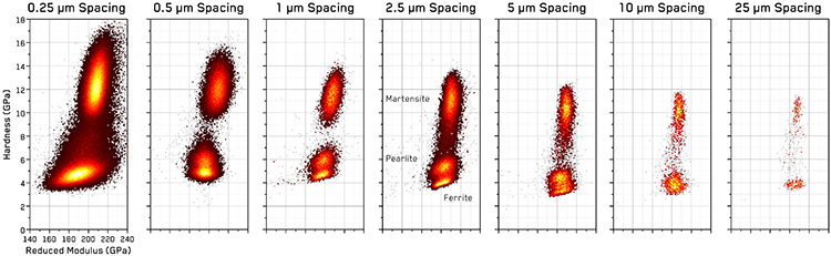 Figure 1. 2D histograms of indentation property distributions as a function of inter-indentation spacing from the maps acquired over the case-hardened C45 steel in cross-section – illustrating the transitions between mapping resolution and phase resolution. Histogram coloring is on an arbitrary scale, due to varying number densities between scales.
These are therefore arbitrary units, depending on the number of total indentations performed. In this study, as the mapping areas were kept constant in rectangular grids (25, 10, 5, and 2.5 µm spacings) and the square grids (1, 0.5, and 0.25 µm spacing), the absolute number of indentations performed at each spacing increment varies significantly: 725 indentations at 25 µm spacing versus 160,000 indentations at 0.25 µm spacing.
These figures offer a simple visual method to evaluate ‘hot spots’ in the indentation property space which statistically correspond to individual phases. As shown in previous work [7], these ‘peaks’ in the 2D histograms often take the form of elliptical, normal distributions which are elongated along the direction of the H/E ratio. In Figure 1, we can observe at least two distinct clusters or hot spots at each map resolution level. The harder of these corresponds to the Martensite-rich portion of the case-hardened steel, while the lower, softer cluster corresponds to the substrate, medium-carbon steel consisting of Pearlite and Ferrite. As visualized in the previous application note, the Pearlite grains are a lamellar composite of Cementite lamella within a Ferrite matrix.
If we examine the 2D histograms in Figure 1 from the largest length scale to the smallest, we initially observe two distinct but low number density clusters at 25 and 10 µm spacings. As we increase the mapping resolution to 5 and 2.5 µm spacing, the cluster peaks become significantly more distinct, and the lower cluster splits as the Pearlite and Ferrite grains become distinct. An increase in intermediate values between the main clusters is also noted with increasing resolution from 25 to 2.5 µm spacing, due to more indentations occurring on phase boundaries between Martensitic and Ferritic grains.
As we examine the transition from 2.5 to 1 µm spacings, it is important to remember that the 2.5 µm spacing map is a rectangular grid covering the entire region of the sample from the edge-hardened Martensite to the substrate, while the 1 µm spacing data (and finer resolutions) is taken from two 100×100 µm square grids in the Martensitic and Pearlitic regions. Therefore, the quantity of intermediate values measured on phase boundaries between Martensitic and Ferritic grains decreases dramatically at 1 µm spacing, due to this dataset being the combination of datasets from distinct regions of Pearlitic substrate steel and Martensitic steel.
At 1 and 2.5 µm spacings, distinct clusters from Martensite, Pearlite, and Ferrite phases are all clearly observed. However, at submicron resolutions, the Pearlite phase becomes less distinct. This is counter to the observations in the maps in the previous notes, where at 0.5, and 0.25 µm spacings, the individual Cementite lamella became more distinct. These two phenomena are related, as the Pearlite phase consists of Cementite and Ferrite lamella. Once sufficient resolution is achieved to distinguish them then the Pearlite ceases to appear as a single cluster/phase. Instead, the clusters become less distinct as the harder Cementite is apparent, but a large fraction of the indentations occur on the phase boundaries between the Cementite and Ferrite lamella.
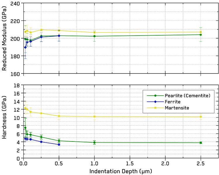 Figure 2. Indentation properties of individual phases extracted from the statistical distributions as a function of indentation depth.
The results of the phase deconvolution using the Gaussian Mixture algorithm from the multi-scale maps are shown in Figure 2. Within the Martensite phase, the reduced modulus is relatively constant with length scale at ~207 GPa. The mean hardness of the Martensite phase is also relatively unaffected by size, only varying from 10 to 12 GPa over 3 orders of magnitude.
Within the substrate steel, the mean reduced modulus remains constant at ~203 GPa at higher indentation depths, until 0.1 µm (1 µm spacing) where the transition from rectangular grids spanning a large area of the sample to local square grids within the Pearlite and Martensite regions occurs. Then the reduced modulus of the Pearlite and Ferrite decreases slightly, possibly due to local variation in the sample. At sub-micron resolutions, the reduced modulus of the Ferrite and Cementite phases begin to become distinct. The hardness of the ferrite phase increases slightly with decreasing indentation depth, while the hardness of the Pearlite/Cementite phase shows a similar trend before increasing more significantly at 0.25 µm spacing due to the harder Cementite becoming distinct from the Pearlite mixed phase.
Conclusion
In this application note, the capability of mechanical microscopy to determine the properties of individual, constituent phases within a complex microstructure was demonstrated using multi-scale mapping across a case-hardened C45 steel cross-section. This required a combination of high precision maps performed at several resolution length scales and statistical deconvolution tools. Gaussian mixture algorithms were successfully employed to determine the mean reduced modulus and hardness of Martensite, Pearlite, and Ferrite phases from indentation property distributions. At the finest scale of 25 nm indentations performed with a 0.25 µm spacing, it was even possible to separate the properties of Cementite lamella within the Pearlite phase. This application of mechanical microscopy to measure constituent phase properties demonstrates the capability of the technique to determine the properties of individual phases within complex microstructures over several different length scales from millimeter to submicrometer.
References
- P.S. Phani, W. Oliver, Materials & Design, 164 (2019) 107563.
- W.C. Oliver, G.M. Pharr, Journal of Materials Research, 7 (1992) 1564-1583.
- F.-J. Ulm, M. Vandamme, C. Bobko, J. Alberto Ortega, K. Tai, C. Ortiz, Journal of the American Ceramic Society, 90 (2007) 2677-2692.
- H. Besharatloo, J.M. Wheeler, Journal of Materials Research, 36 (2021) 2198-2212.
- E. Rossi, J.M. Wheeler, M. Sebastiani, Current Opinion in Solid State and Materials Science, 27 (2023) 101107.
- T. Hastie, R. Tibshirani, J.H. Friedman, The Elements of Statistical Learning: Data Mining, Inference, and Prediction, Springer, 2001.
- J.M. Wheeler, Journal of Materials Research, 36 (2021) 94-104.

