Tags: Mechanical Microscopy, High-Temperature Nanoindentation, Correlative Mechanical Microscopy
Operando mechanical microscopy allows the mechanical properties of a microstructure to be assessed in conditions similar to those they would experience in service, e.g. high or low temperatures. This is often challenging for load-controlled systems, as thermal softening of different phases prevents consistent indentation sizes for mapping. Using displacement-controlled indentations allows consistent indentation and map sizes at any temperature. In this application note, operando mechanical microscopy is applied in a combinatorial investigation of the Ni—Mo system at temperature up to 500 °C. This allowed the temperature-dependent mechanical properties of the primary phases and solid-solution regions to be determined. This demonstrates the potential of the operando, correlative approach for combinatorial investigations.
Introduction
High temperature nanoindentation is a very attractive technique for the determination of the temperature dependence of a wide variety of mechanical properties [1]. Using high-speed, displacement-controlled nanoindentation at elevated temperatures, we can perform operando mechanical microscopy to determine the temperature-dependence of microstructures in a visual, statistical, and quantitative fashion.
This is a very attractive technique, as it allows consistent sampling of the microstructure at various temperatures with a uniform indentation size, regardless of differences in local composition, hardness, or thermal softening. High-speed, local measurements are particularly desirable for investigating properties in high temperature testing, where faster measurements both reduce any possible influence of thermal drift and allow for greater statistical sampling.
In this application note, operando mechanical microscopy is performed in a combinatorial investigation of the Ni—Mo system [2]. This allowed the temperature-dependent properties of a wide range of compositions to be investigated in a single study. Details of the approach are described, particularly the system concerns, and the ability of the correlative approach to identify individual phases is demonstrated and discussed. Temperature-dependent properties are compared with literature values for phases where available.
Experimental Considerations
High Temperature Operation
For high temperature testing, several technical features are required to allow testing to be performed in conditions similar to room temperature. Ideally, a system operated at high temperatures should behave identically to how it performs under ambient conditions with a similar degree of ease of use, no changes in dynamics or noise, and stable performance over long test periods. To achieve this, the high temperature module of the NMT04 In-Situ SEM Nanoindenter was designed with a number of features.
The low thermal mass of the heated portion of the indenter tip on the MEMS heater allows the tip to be rapidly matched with the sample surface temperature using an automated procedure. This consists of performing a series of surface find procedures, where the indenter is rapidly brought into contact with the surface and briefly held there at a constant force. Any deviations in displacement during the hold period are noted and used to align the tip and surface temperature. The tip is then retracted and the procedure repeats until the user is satisfied with the degree of alignment. This procedure automatically accounts for thermal expansion of the system components, as it effectively follows the sample surface through a series of surface finds and retractions.
This combination of precisely-aligned indenter and sample temperatures and stable thermal gradients within the surface frame are essential for achieving low thermal drift (displacement changes due to thermal expansion) during measurements.
Displacement Control
In order to achieve a regular map, mechanical microscopy requires that the indentations within the grid have a uniform size, i.e. performed to the same depth. In load control, the load must be carefully chosen to ensure that the spacing is proportional to the indentation produced in the softest phase in the map. Otherwise, indentations in the soft region will overlap with its neighbors. This means for indentations maps performed in load control, a significant disparity in indentations depths and spacings can be expected for maps over dissimilar phases.
At high temperatures, this becomes even more challenging, as metallic phases may significantly soften faster than reinforcing intermetallic phases due to thermal softening. This makes displacement control an essential feature for a system to perform operando mechanical microscopy.
Sample Preparation
To generate a combinatorial library for investigation of the Ni—Mo system (Figure 1), a diffusion couple was produced. Nickel and Molybdenum bars (99.99%, Zhongnuo New Materials Ltd.), both of about 1 cm in length, were gently compressed at 150 MPa and subjected to 900 °C in vacuum using the Gleeble 3500 dynamic testing system. Afterward, the Ni–Mo junction was encapsulated in an argon-purged Quartz tube and annealed at 1200 °C for 168 h, followed by a water quench. This rapid quench from high temperature avoids the formation of Ni4Mo and Ni3Mo intermetallic phases. However, precipitation of these phases may occur at elevated temperatures.
![Phase diagram of the Ni—Mo system [2] with phases shaded and diffusion temperature indicated.](https://www.oxinst.com/learning/uploads/inline-images/ni-an23-fig1-750-20250530095359.png) Figure 1. Phase diagram of the Ni—Mo system [2] with phases shaded and diffusion temperature indicated.
Figure 1. Phase diagram of the Ni—Mo system [2] with phases shaded and diffusion temperature indicated.
The sample was sectioned using an alumina cut-off wheel (Struers 50A 13), then metallographically prepared using successively finer diamond abrasives, finishing with a 60 nm SiO2 particle suspension.
Indentation Procedures
Mechanical microscopy was performed using an FT-I04 Femto-Indenter (FemtoTools AG, Switzerland) with a diamond Berkovich indenter. Each indentation was conducted in ~1 s with a ramped oscillation amplitude at a frequency of 100 Hz. Total time for each indentation including repositioning was ~2.5 seconds. Each indentation was performed to a specified depth of 200 nm in the interdiffusion zone, so that a spacing of 4 µm between indentations could be used while still ensuring an indentation depth/spacing ratio of 20 was maintained [3].
Testing was performed at ambient temperature and increasing increments of 100 °C up to 500 °C. During each temperature ramp, tip temperature matching was performed using the procedure described earlier. Higher temperature mapping was not performed due to indenter-sample reactions [4].
Microstructural analyses were performed using analytical SEM, backscattered electron (BSE) imaging, and combined EDX-EBSD mapping in a Hitachi SU-5000 (Oxford Instruments UltimMax 100 EDX and Unity BEX detectors) at 20 kV.
Results
Sample Characterization
The Ni—Mo diffusion couple displays a wide solid-solution region within the Nickel phase with Molybdenum contents of up to ~25% over ~400 µm of distance from the interface with the δ-NiMo intermetallic phase - Figure 2. As expected from the phase diagram in Figure 1 [2], very limited Nickel contents are observed within the Molybdenum phase on the right.
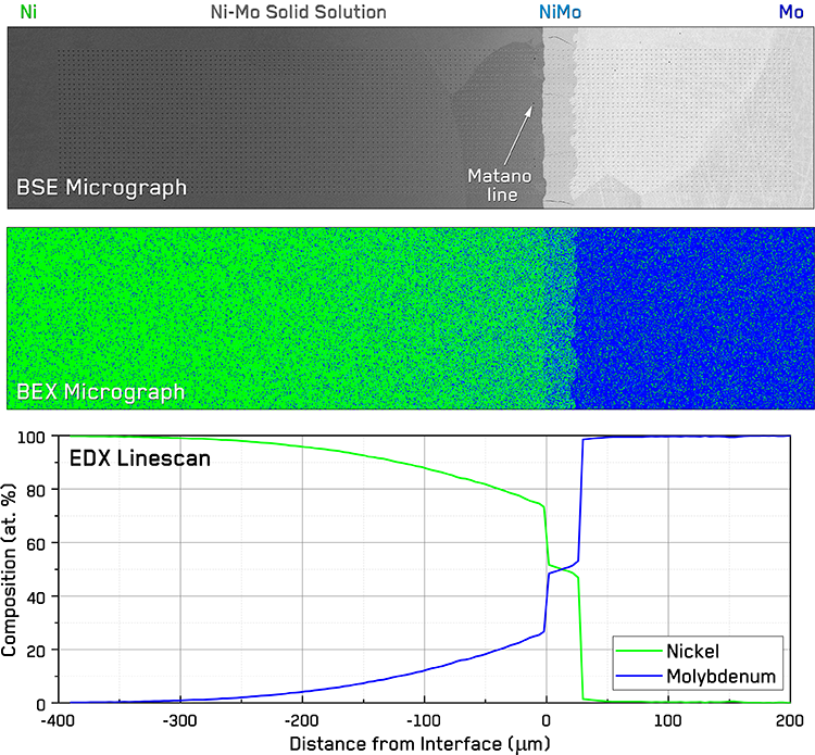 Figure 2. Characterization of the Ni-Mo diffusion couple over the region where the 300° C map was performed.
The Matano line, indicating the original interface between the two metals is observed as a line of fine porosity near the NiMo intermetallic. The majority of the Nickel phase consists of extremely large grains with a few smaller grains near the interface, while the Molybdenum phase contains a somewhat finer but still large grain structure. Compositional ranges for the various phases are in good agreement with the ranges observed at the diffusion temperature within the phase diagram - Figure 1.
Operando Mechanical Microscopy
The operando mechanical microscopy maps obtained at different temperatures in the interdiffusion zone of the Ni—Mo couple are shown in Figure 3. Excellent visual correlation is observed between the overlays of the hardness maps with the BSE micrographs of the regions. The hardness maps clearly trends that mirror the compositional variations observed in Figure 2 with hardness increasing with Molybdenum content within the Nickel solid solution region of the sample, a distinct NiMo intermetallic phase, and then the Molybdenum phase on the right.
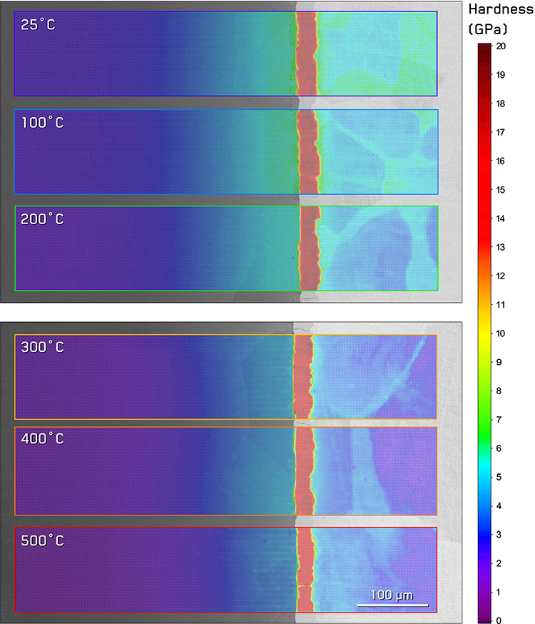 Figure 3. Hardness maps overlaid on back-scattered electron micrographs of adjacent regions of the Ni—Mo diffusion junction acquired at temperatures from 25 to 500 °C.
Hardness maps acquired at temperatures from 25 to 500 °C are overlaid on the BSE micrographs from the two tested regions. A single, continuous regions of sufficient size for all maps was not available on the sample due to previous tests.
Hardness values can be observed to decrease within increasing temperatures at different rates between the various phase regions within the sample. The Nickel solid solution region smoothly decreases in Hardness with temperature, which can be seen as the solid solution region appearing to shift towards the right with a color shift. The NiMo intermetallic appears rather temperature insensitive, and the Molybdenum phase shows an initial rapid decrease up to 300 °C with steady properties afterwards.
Correlated Cluster Analysis
For statistical analysis of the temperature dependence of the various phases from the mechanical microscopy data, it is helpful to examine the property distributions in a compositionally-labeled 2D scatter plot - Figure 4. Similar to previous work on Ni-Ta [5], this shows the property clusters of the various phases with color-coding according to their Molybdenum content. On the left, a linear stripe with purple-blue shading corresponds to the Nickel solid-solution region, with a secondary cluster at the top corresponding to a different grain near the intermetallic interface. This difference in grain orientation causes a shift in reduced modulus, due to elastic anisotropy, but the increasing hardness trend with Molybdenum content (up to ~25%) is continued. The green cluster at the top is the NiMo intermetallic, while the dark red clusters are the various grains of near-pure Molybdenum.
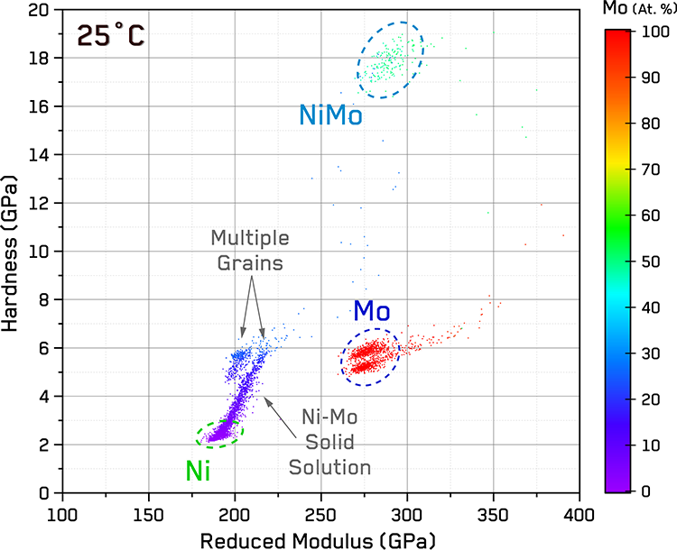 Figure 4. 2D scatter plot showing hardness as a function of reduced modulus from room temperature mechanical microscopy results with datapoints color-coded using correlated EDX to illustrate compositional gradients and primary phases.
2D scatter plots are useful for plotting the compositional variation using color-coding, but overlapping points prevent them from giving a statistical impression of the cluster’s “density” in terms of precision in properties.
This is easily visualized using a 2D histogram - Figure 5. As shown in previous work [5], this type of plot shows the number of indentations fitting within a fixed bin of H and E values such that phases appear as clusters or peaks.
To track this and determine the temperature dependence of the properties of the various phases, we employed Mixed Gaussian clustering algorithms. The number of clusters fitted was varied for different phases to achieve fits of the individual pure phases (Ni and Mo without significant alloying content). For Ni, this required a surplus of clusters, which segmented the elongated Nickel solid solution cluster into several clusters, one of which correspond to the bright peak of the ‘pure’ phase (Figure 5), while other Ni clusters captured the solid solution range and individual grains near the intermetallic interface. To capture the Mo phase, only 4 clusters were used, forcing the software to segment the data into the three primary phases with one additional cluster for outliers. This effectively grouped the clusters from the various grains in the Molybdenum phase (Figure 5) into a single averaged cluster for analysis.
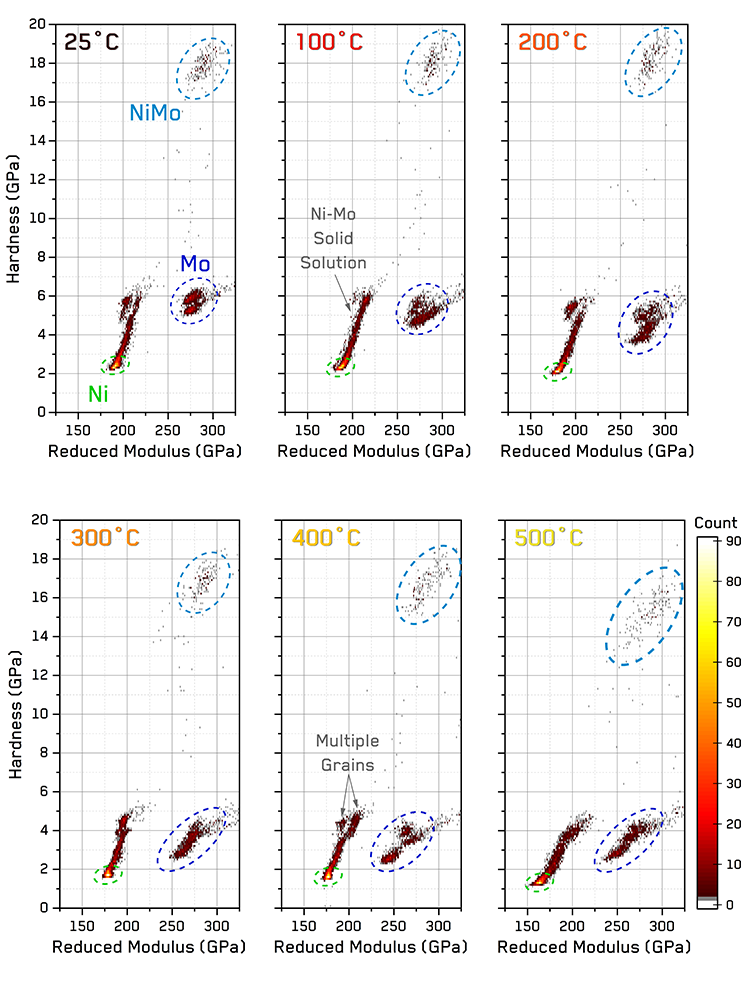 Figure 5. 2D histograms from operando mechanical microscopy measurements as a function of increasing temperature up to 500 °C with phases and features of interest labeled. Sample numbers and counts per 2D bin are consistent for each temperature for comparison.
Similar property distributions in terms of shape and relative location are observed in all temperatures, suggesting that new phases did not precipitate or arise through transformation at elevated temperatures. The absolute positions of the clusters, however, do shift with increasing temperature. Results of the Mixed Gaussian clustering as a function of temperature are shown in Figure 6.
Trends in reduced modulus in Figure 6 show good agreement with literature values for the primary metallic phases. Literature values from Köster [6] and Dreshpak [7] were measured using acoustic techniques. Some variation from literature values are seen in the current measurements, which is likely attributable to anisotropy between various grains. High temperature modulus values were not available for the NiMo phase.
Hardness trends for the Nickel phase as a function of temperature are observed to be consistent with those of Minnert et al. [8], though their indentations were performed to a depth of several microns. Comparable literature values for nanoindentation hardness were not available for the Mo and NiMo phases. Significantly larger hardness variation is observed in the Mo phase compared to the Ni phase, which is in agreement with the larger scatter seen in the 2D histograms from the various clusters from different grain orientations - Figure 5.
This successfully demonstrates the capability of operando mechanical microscopy to determine the temperature-dependent properties of various phases within a microstructure. This is easily combined with analytical electron microscopy for correlated techniques to determine the temperature-dependence of individual microstructural phases such as grains of a particular orientation, specific crystallographic phases, types of grain boundary, or solid solution compositional ranges. Applying this technique in a combinatorial manner allows a large number of compositions and phases to be interrogated simultaneously, as demonstrated here.
![Hardness and reduced modulus of the primary phases in the Ni—Mo diffusion couple compared to literature values [6-8].](https://www.oxinst.com/learning/uploads/inline-images/ni-an23-fig6-750-20250530095908.png) Figure 6. Hardness and reduced modulus of the primary phases in the Ni—Mo diffusion couple compared to literature values [6-8].
Figure 6. Hardness and reduced modulus of the primary phases in the Ni—Mo diffusion couple compared to literature values [6-8].
Conclusions
In this application note, operando mechanical microscopy was demonstrated at high temperatures in a combinatorial investigation of the Ni—Mo system. High temperature nanoindentation maps using consistent parameters were performed on adjacent regions of a Ni—Mo diffusion couple. This allowed mechanical property maps to be acquired as a function of temperature up to 500 °C. These were observed to correspond perfectly in morphology with backscattered electron micrographs of the investigated regions. This validates that maps were performed with indentation depths and positions consistently at all temperatures. This is only possible using systems with a high degree of thermal stability at temperature and displacement control to perform indentations to a specified depth, regardless of thermal softening. Cluster analysis using a Mixed Gaussian approach was applied to track the statistical properties of the main phases as a function of temperature. Both hardness and reduced modulus values for the primary phases were found to be consistent with literature values for phases where such data were available. By performing these tests on a combinatorial gradient sample (i.e. a diffusion couple), a wide range of compositions and phases were simultaneously characterized as a function of temperature. This demonstrates the potential of this operando, correlative approach for combinatorial investigations.
Acknowledgements
The author gratefully acknowledges the contributions of the groups who assisted in these measurements. Dr. Indranil Basu of Prof. Loffler’s Laboratory of Metal Physics at ETH Zurich performed the EDX characterization.
References
- J.M. Wheeler, D.E.J. Armstrong, W. Heinz, R. Schwaiger, Current Opinion in Solid State and Materials Science, 19 (2015) 354-366.
- H. Okamoto, Journal of Phase Equilibria, 12 (1991) 703-703.
- P.S. Phani, W. Oliver, Materials & Design, 164 (2019) 107563.
- J.M. Wheeler, J. Michler, Review of Scientific Instruments, 84 (2013) 101301.
- J.M. Wheeler, B. Gan, R. Spolenak, Small Methods, 6 (2022) 2101084.
- W. Köster, International Journal of Materials Research, 39 (1948) 145-158.
- V. Dreshpak, Strength of Materials, 1 (1969) 669-670.
- C. Minnert, W.C. Oliver, K. Durst, Materials & Design, 192 (2020) 108727.

