Mechanical microscopy allows the mechanical properties of a microstructure to be assessed as a function of processing conditions. This allows the evolution of microstructures after a series of different heat treatment to be assessed in terms of its phases and their properties. In this application note, mechanical microscopy is applied to investigate the properties of a high chromium, cast iron (HCCI) after a series of heat treatments designed to optimize their properties. The phase-level properties of the resulting microstructures were evaluated using statistical and clustering approaches. This demonstrates the potential of the mechanical microscopy for the evaluation of thermal processing on microstructures.
Introduction
Mechanical microscopy allows the relationships between microstructure, properties, and processing to be characterized in exciting new ways. Since microstructure and properties are directly investigated on the micro-scale by this technique, it provides unique insights into how individual microstructural phases and their properties evolve during processing, such as heat treatments.
High chromium cast irons (HCCI) are an important alloy series for mining and manufacturing applications due to their excellent erosion performance due to their high hardness and corrosion resistance [1]. This arises from the high chromium content preventing the formation of graphite or cementite phases and instead promoting the formation of hard eutectic carbides. Depending on the composition and heat treatments, the microstructure of these cast irons consists of an Austenitic or Ferritic/Martensitic matrix with rod-shaped eutectic M7C3 or M23C7 carbides.
In this application note, we demonstrate the ability of Mechanical Microscopy to characterize the properties of individual phases within HCCIs as a function of thermal processing. This allows the properties of the constituent phases within the microstructure to be determined and analyzed. This requires a combination of high precision to differentiate the phases and statistical analysis for segmenting the data to determine individual phase’s properties. In this work, we compare the performance of statistical and machine learning analysis for the determination of phase-level properties within HCCIs after a series of heat treatments.
Experimental Considerations
Sample Preparation
An HCCI alloy containing 2.53 wt.% C, 26.6 wt.% Cr and other minor alloy elements was prepared for this work using a series of heat treatments [2]. The samples were cut into pieces 20×20×10 mm using an abrasive disc. Four different treatments were applied, as schematically illustrated in Figure 1. First, an As-cast sample is used as a reference. Then, destabilization and a multi-step heat treatment were applied to the samples. For the destabilization process, the samples were heated until 980 °C with a heating rate of around 0.25 °C/s. The specimen was held at the maximum temperature for two different times; 0 and 90 min and subsequently quenched in water.
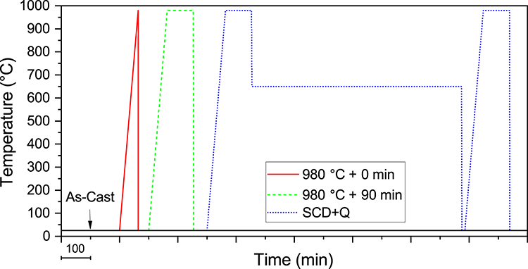 Figure 1. Schematic of the four different heat treatments performed on the HCCI samples.
The multi-step HT (sample SCD+Q) includes a destabilization at 980 °C for 90 min followed by a sub-critical diffusion step at 650 °C for 12 h and quenching in water. A third step includes a second destabilization process at 980 °C for 90 min and quenching. For further details on the multi-step HT, refer to [3].
Prior to the microstructural and mechanical characterization at the submicrometric length scale, the specimens were embedded in conductive resin and subsequently chemo-mechanically polished (CMP) until reaching a mirror-like surface.
Indentation Procedures
Mechanical microscopy was performed using an i04 Femto-Indenter with a diamond Berkovich indenter. Nanoindentation maps of 200 x 150 indents were performed on each sample using a FT-S20,000 sensor. Each indentation was performed using a continuous stiffness measurement (CSM) method in displacement control mode. The indentations were each performed in ~ 1 s with an oscillation frequency of 150 Hz and an amplitude that linearly increased from 0.5 to 2.5 nm with increasing depth. The total time for each indentation including repositioning was ~ 2.5 seconds. Each indentation was performed to a specified depth of 190 nm, so that a spacing of 2 mm between indentations could be used while still ensuring an indentation depth/spacing ratio of 10 [17]. This avoids any significant interaction between neighboring indents. Hardness (H) and reduced elastic modulus (Er) were measured as a function of depth for each location, and representative values for each were taken by averaging values from depths > 150 nm to minimize the influence of indentation size effects for hardness values and > 100 nm for modulus values.
Phase Quantification
The phases contained in each of the samples were previously identified [4, 5] by X-ray diffraction (XRD) using a PANalytical Empyrean diffractometer system equipped with a Bragg Brentano-HD (BBHD) module and an ultra-fast PIXcel3D detector. Additionally, the volume fraction of the Retained Austenite was estimated by the Rietveld refinement approach, using the software Material Analysis Using Diffraction (MAUD) [6].
To segment the large, multidimensional datasets that result from mechanical microscopy, a variety of statistical and clustering approaches have been developed. The most commonly applied method was developed by Ulm et al. [7], which fits a series of Gaussian peaks to a property distribution. However, this method only analyzes properties individually, not their interrelationships. This can make it challenging to determine which pairs of peaks from different properties correspond to a given phase. For example, if two phases had different hardness values, but similar modulus values, the Ulm method would not help determine which modulus peak value corresponds to which phase.
Newer multidimensional analysis methods allow data segmentation of multiple properties at the same time [8], precluding this issue. A recent review of the various statistical and machine learning approaches to segmenting indentation data is available [9]. Oxford Instruments Nanoindentation analysis software features two multidimensional clustering algorithms [10] for segmenting data for phase-level property determination: k-means and Gaussian Mixture.
In this work, we applied the Gaussian Mixture algorithm to determine the phase properties of each property distribution. This algorithm models the data as independent observations from a mixture of bivariate normal distributions. An expectation maximization algorithm finds the mean and covariance matrices for the normal distributions which best fit the overall property distributions. This method can segment clusters which strongly differing in size or areal fraction. Further, it is suitable segmenting data where the fitting parameters are correlated.
In some cases, an additional ‘interphase’ cluster was included to account for indentations which were located on phase boundaries and gave intermediate results. This allowed for more accurate fitting of the property distributions.
Results
Sample Characterisation
The evolution of the HCCI samples’ microstructures and their properties with heat treatment is shown in a series of 2D histograms and accompanying H/Er ratio overlays on backscattered electron micrographs - Figure 2.
As shown in previous work [11], 2D histogram plots show the number of indentations fitting within a fixed bin of H and Er values such that phases appear as clusters or peaks. This provides an easy, visual method of evaluating the statistical distribution of phase properties in terms of both H and Er values simultaneously. This provides a visual method for evaluating the effectiveness of statistical methods of machine learning clustering algorithms. Both the locations and standard deviations determined by one-dimensional Ulm statistical deconvolution and two-dimensional mixed Gaussian clustering algorithms are shown on the 2D histogram plots, as well as the approximate regions in property space occupied by the primary phases.
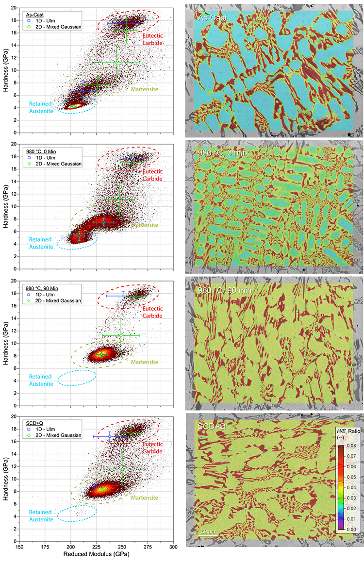 Figure 2. 2D histograms and H/Er ratio maps showing the evolution of the microstructures and their properties as a function of heat treatment with the phase regions labeled and statistical/cluster locations and standard deviations.
Moving through the heat treatments in order, we can see a clear evolution in properties and microstructure between the As-cast and SCD+Q states. In the As-cast state, we can see a very pronounced cluster corresponding to the Retained Austenite phase, which is visible as the ‘blue’ regions in the H/Er ratio overlays. A second, very hard cluster is also observed, corresponding to the Eutectic Carbide phase, shown in ‘red’. These carbides can be seen to be surrounded by a thin layer of ‘gold’ Martensite, which is seen as a diffuse cloud of datapoints rising from the Retained Austenite cluster to higher hardness and reduced modulus values.
In the second condition, after a short destabilization treatment (980 °C for 0 min), it can be immediately seen that the amount of Retained Austenite has significantly decreased. This is visible in both the reduced peak intensity in the histograms and the lower amount of ‘blue’ regions in the micrograph. However, the amount of the Martensite phase has significantly increased. Eutectic carbides appear to be reduced in size and quantity.
In the third condition, after a longer destabilization treatment (980 °C for 90 min), we can observe that almost no Retained Austenite appears to remain, and the microstructure now consists solely of Eutectic Carbides and Martensite. This is very clear in the 2D histogram, where only two distinct clusters remain.
Finally, in the fourth condition after destabilization and sub-critical diffusion steps, we observe a very similar microstructure and property distribution to the third condition. However, the property distributions show a much greater amount of datapoints between the two main clusters for Martensite and Eutectic Carbide. This suggests the presence of a fine admixture of the two phases, where indentations are occurring on both phases simultaneously in many places.
Comments on Statistical Deconvolution and Clustering Results
Figure 2 also shows the locations and standard deviations identified using the statistical deconvolution methods of Ulm et al. and using a Mixed Gaussian clustering algorithm. The Ulm et alia method deconvolutes the hardness and reduced modulus distributions separately, while the Mixed Gaussian method clusters in both properties simultaneously. It must also be noted that the Mixed Gaussian algorithm is automated and unsupervised, whereas the statistical convolution must be performed by a skilled operator.
In most cases, both methods are able to correctly identify, relative to the 2D histogram peaks, the locations and properties of the main phases in the heat treatments. Close overlap is frequently seen between peaks identified using both methods. Both methods also sometimes are required to use ‘extra’ peaks or distributions to fit ‘interphase’ regions, where indentations are assumed to have occurred on two phases simultaneously. These often appears a clouds of datapoints connecting two peaks within a 2D histogram. Which peaks are connected by these clouds is indicative of which phases share an interface. In the As-cast state, all three peaks can be seen to be connected. However, in the second condition, (980 °C for 0 min), the Retained Austenite no longer share interfaces with the Eutectic Carbides. This is supported by the micrograph, which now shows there to be Martensite surrounding the carbides.
Multi-dimensional analyses are advantageous when there is significant property overlaps in one dimension. This can be most clearly seen in the final heat treatment condition, where the 2D method correctly identifies the center of both Martensite and Eutectic Carbide clusters in terms of both hardness and reduced modulus. However, the 1D method is only able to correctly identify the positions in terms of Hardness. The size of the Martensite peak in reduced modulus, combined with the close overlap in values, overwhelmed the smaller Eutectic carbide peak causing the deconvolution to misidentify the reduced moduli of the two phases.
Phase-level Properties
A more conventional way of presenting the deconvoluted/clustered data shown overlaid on the 2D histograms shown in Figure 2 is given below in Figure 3, where the phase-level properties of each phase as determined by the two methods are shown for each heat treatment. As seen in Figure 2, the two methods are generally in good agreement. The only real disparities are seen in the last two heat treatments for the Eutectic Carbide phase, where the one-dimensional method underestimates the reduced modulus of the cluster.
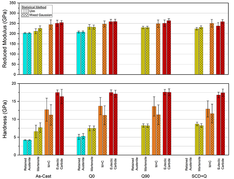 Figure 3. Phase-level properties as a function of heat treatment and segmentation method.
This good agreement between the two methods validates the performance of the unsupervised, Mixed Gaussian clustering algorithm in comparison to the more labor-intensive statistical deconvolution method.
Conclusions
In this application note, mechanical microscopy was demonstrated to characterize the influence of thermal processing on the evolution of a high chromium cast iron’s microstructure. The applied heat treatment destabilization heat treatment was able to successfully remove nearly all undesired Retained Austenite from the matrix while promoting a Ferritic/Martensitic matrix and Eutectic Carbide hard phases. This requires a combination of high precision to differentiate the phases and analysis for segmenting the data to determine individual phase’s properties. Two analyses using a conventional statistical deconvolution (Ulm’s method) and a machine-learning-based Mixed Gaussian clustering approach were applied to track the statistical properties of these main phases after a series of heat treatments. Both hardness and reduced modulus values from the Mixed Gaussian clustering of the primary phases were found to be consistent with conventional statistical deconvolution methods. In a few cases, the 2D cluster analysis was found to give superior results, particularly in terms of reduced modulus, to the 1D conventional method. This demonstrates the potential of mechanical microscopy for monitoring the evolution of individual phases and their properties during thermal processing stages.
References
- G. Laird, R.B. Gundlach, K.K. Röhrig, K.E. Frink, Abrasion-resistant cast iron handbook, American Foundry Society, Des Plaines, 2000.
- U.P. Nayak, M.A. Guitar, F. Mücklich, Metals, 10 (2020) 30.
- M.A. Guitar, S. Suárez, O. Prat, M. Duarte Guigou, V. Gari, G. Pereira, F. Mücklich, Journal of Materials Engineering and Performance, 27 (2018) 3877-3885.
- U.P. Nayak, F. Mücklich, M.A. Guitar, Metals and Materials International, 29 (2023) 934-947.
- M.A. Guitar, U.P. Nayak, D. Britz, F. Mücklich, International Journal of Metalcasting, 14 (2020) 755-765.
- L. Lutterotti, Nuclear Instruments and Methods in Physics Research Section B: Beam Interactions with Materials and Atoms, 268 (2010) 334-340.
- F.-J. Ulm, M. Vandamme, C. Bobko, J. Alberto Ortega, K. Tai, C. Ortiz, Journal of the American Ceramic Society, 90 (2007) 2677-2692.
- H. Besharatloo, J.M. Wheeler, Journal of Materials Research, 36 (2021) 2198-2212.
- E. Rossi, J.M. Wheeler, M. Sebastiani, Current Opinion in Solid State and Materials Science, 27 (2023) 101107.
- T. Hastie, R. Tibshirani, J.H. Friedman, The Elements of Statistical Learning: Data Mining, Inference, and Prediction, Springer, 2001.
- J.M. Wheeler, B. Gan, R. Spolenak, Small Methods, 6 (2022) 2101084.

