Correlative mechanical microscopy of combinatorial libraries is an enabling technology for high-throughput investigations. This allows investigations of thousands of multi-element combinations in a single experiment. The advantage of this high-throughput approach over conventional approaches increases by an order of magnitude with the number elements simultaneously investigated. In this application note, this technique was applied to determine the alloying effects of W, Ti and Ta on the microstructural and mechanical properties of Co-20Ni-7Al-8W-4Ti-1Ta superalloys. A combinatorial library was generated using a carefully-designed diffusion-multiple to provide a large compositional space for investigation. A combination of electron microscopy image analysis, quantitative compositional analysis, and high-speed nanoindentation was performed to determine quantitative relationships between microstructure, alloy composition, and mechanical properties using correlated datasets. An optimized compositional range was determined from these high-throughput results to achieve a balance between low density, high γʹ area fraction, and mechanical properties. This demonstrates the potential of correlative mechanical microscopy for the high-throughput investigations of complex alloys.
Introduction
Superalloys are key high-temperature structural materials for aeroengine and gas turbine applications [1]. To date, Ni-base alloys are the most widely-used class of superalloys due to their excellent combination of high-temperature mechanical and environmental capabilities [2]. However, further increases in the application temperature range of Ni-base superalloys to increase engine efficiency is challenging to achieve, as these temperatures approach the γ′ solvus temperatures of these alloys [3]. Therefore, a new generation of high-temperature structural materials is urgently needed to improve aeroengine and gas turbine efficiency to meet environmental targets.
A strong candidate for this is multi-component CoNi-base superalloys, strengthened by coherent L12-structured γ′ precipitates, due to their excellent combination of properties balanced by microstructure stability, mechanical property and oxidation resistance [4-9]. However, conventional testing and alloy development approaches are expensive and time consuming due to the complex compositions of these alloys, which often require a precise blend of 6 or more elements – creating an enormous multi-dimensional compositional space.
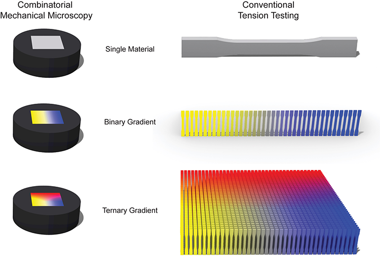 Figure 1. Schematic illustration of the advantage of high-throughput, combinatorial testing of single samples with compositional gradients versus conventional serial testing of large numbers of individual compositions.
To meet this challenge, a high-throughput experimental approach is required: Correlative mechanical microscopy of combinatorial libraries. This investigates a wide, multi-component compositional range within a single sample with minimal experimental efforts. This allows the relationships between alloy composition, microstructure, and mechanical properties to be determined in a multi-dimensional compositional range [10, 11]. Using correlated datasets, the relationships between microstructure, composition, and properties can be deconvoluted even in complex multicomponent alloys. This type of high-throughput experimental approach promises to significantly accelerate the exploration of alloying influences in multi-component alloy systems.
In this study, high-throughput correlative mechanical microscopy was employed on a superalloy diffusion-multiple to systematically investigate the alloying effects of W, Ti, and Ta on the microstructure and mechanical properties of a model Co-20Ni-7Al-8W-1Ta-4Ti alloy. Correlated datasets of nanoindentation, compositional, and microstructural analysis results were obtained on a ternary junction within the diffusion multiple. From these results, quantitative relationships between composition, microstructure and mechanical properties were established in a large compositional space. This investigation demonstrates the significant advantages of high-throughput correlative mechanical microscopy for the development of multi-component alloy systems.
Experimental Considerations
Necessity for High Throughput
With the increasing complexity of modern alloys, a large multi-dimensional compositional space exists for each alloy. Superalloys have a large number of elemental components whose compositions are precisely adjusted within fractions of a percent. This results in an extremely large number of possible combinations of elements. If we consider the simpler case of alloys made of three elements, where the composition is allowed to vary by 1%. The sum of the percentages of all elements must equal 100%, so xA+xB+xC = 100. The formula for the number of solutions in such a case is
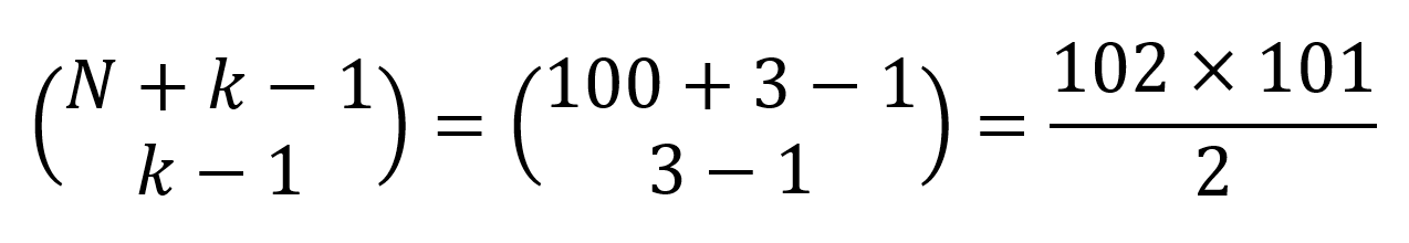 so that with only three elements, where the composition of each element can vary by 1%, is 5,151.
If we decrease the composition increment to 0.1%, then the number of combinations increases by two orders of magnitude to 501,001 combinations. For a six element Superalloy, where the composition of each element can vary by 0.1%, the number of alloy compositions is nearly 85 Trillion.
These numbers are obviously impractical for conventional experimental investigations. However, high-throughput combinatorial approaches may make a significant fraction of these combinations accessible. Figure 1 shows the advantage of performing mechanical microscopy on samples with a combinatorial gradient over serial conventional testing of individual alloy compositions.
As the number of elements increases, the power of the technique increases exponentially. By testing a ternary junction with a relatively small 40×40 grid, over 1600 compositions could be investigated. With large grids, millions of compositions could be investigated in a single experiment.
Sample Preparation
A multi-component diffusion-multiple was carefully designed using a base model alloy Co-20Ni-7Al-8W-1Ta-4Ti (at.%) and eight other senary or septenary alloys, as shown in Figure 2. Previous studies on this diffusion-multiple have been published in Refs. [12, 13]. In order to further explore the interactive effects of W, Ti and Ta on microstructure and properties, the triple junction marked by red circle in Figure 2 was investigated in this study. This triple junction consisted of three alloys: the Base alloy and the 5Ta4W and 10Ti2W alloys, which are enriched in W, Ta, and Ti, respectively.
It is worth mentioning that the total contents of W, Ti, and Ta in these three alloys were maintained at 13 at.%. This compositional design provides continuous variations of W, Ti, and Ta contents over a considerable compositional space within the triple junction region.
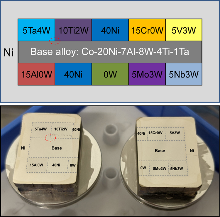 Figure 2. Schematic and photograph of diffusion multiple samples with junction of interest circled in red.
The component alloys of the diffusion-multiple were prepared by arc melting high purity metals under an argon atmosphere. The designed sizes of these alloy blocks are far larger than the expected maximum diffusion distances, in order to prevent interactions between neighboring diffusion junctions. Before assembly, segments were grinded using SiC paper up to 2000 grit and sonicated in pure ethanol to ensure clean, relatively flat interfaces. Then the alloy segments were assembled according to the schematic in Figure 1 and encase in a pure Ni cartridge.
The specimen was then encapsulated in an evacuated quartz tube which was backfilled with argon gas. After that, a two-stage heat treatment was performed, including a solution treatment conducted at 1250 °C for 24 h and a subsequent long-term aging treatment at 1000 °C for 1000 h. After the heat treatment, the specimen was subsequently water-quenched to retain the microstructure at 1000 °C at ambient temperature. The heat-treated diffusion-multiple was then sectioned and prepared using standard metallographic techniques.
Nanoindentation
Mechanical microscopy was performed using an FT-I04 Femto-Indenter (FemtoTools AG, Switzerland) with a diamond Berkovich indenter. Nanoindentation maps of 256 x 200 indents were performed on each sample using a FT-S20,000 sensor. Each indentation was performed using a continuous stiffness measurement (CSM) method in displacement control mode. The indentations were each performed in ~ 1 s with an oscillation frequency of 140 Hz and an amplitude that linearly increased from 0.5 to 2.5 nm with increasing depth. The total time for each indentation including repositioning was ~ 2.5 seconds. Each indentation was performed to a specified depth of 190 nm, so that a spacing of 2 mm between indentations could be used while still ensuring an indentation depth/spacing ratio of 10× [17]. This avoids any significant interaction between neighboring indents. Hardness (H) and reduced elastic modulus (Er) were measured as a function of depth for each location, and representative values for each were taken by averaging values from depths > 150 nm to minimize the influence of indentation size effects for hardness values and > 100 nm for modulus values.
Composition and Microstructure
The quantitative compositional analysis of the diffusion junction was determined using a JEOL JXA8230 with an accelerating voltage of 20 kV and a probe current of 10 nA. Composition maps were collected over the triple junction with a step size of 25 μm, spanning a 325×325 μm2 region. The beam diameter of each spot was set as a circle with a diameter of 10 μm to determine the average alloy composition of the local area rather than point locations.
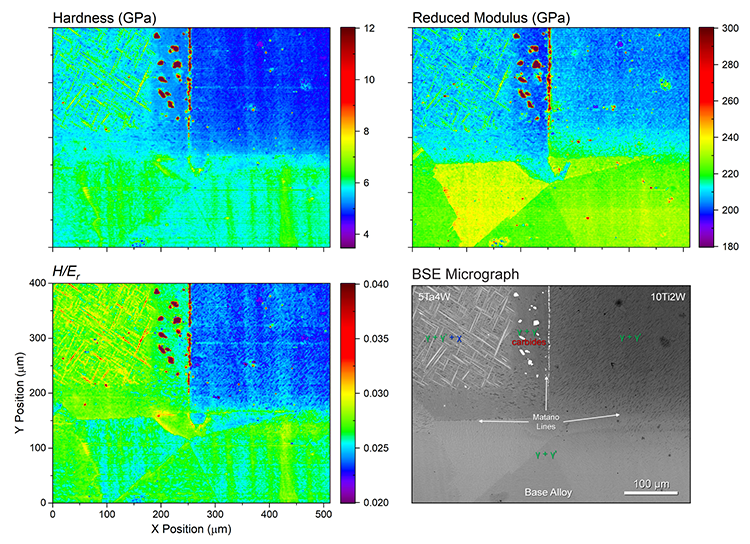 Figure 3. High-speed nanoindentation property maps of the investigated triple junction region: (a) hardness, (b) reduced modulus, and (c) H/Er.
To investigate the local microstructure, the specimen was etched for 20 s with a solution of 33% HNO3, 33% HCl and 34% H2O. Microstructural characterization was performed using a ZEISS SUPRA 55 field-emission scanning electron microscope (FE-SEM) in both backscattered electron (BSE) and secondary electron (SE) imaging modes. Phase identification was performed using combined compositional analysis (with default beam spot). In order to establish a quantitative relationship between composition and microstructure, the SEM image of the investigated triple junction was divided into 196 areas, each corresponding to a region in the compositional analysis grid. The area fractions of γ′, χ, and carbide phases in each area were quantitatively analyzed using Image-Pro software (Media Cybernetics, USA).
Results
The results of this investigation are threefold: mechanical property, microstructural, and compositional variation over the ternary junction. Mechanical property variation over the Base-5Ta4W-10Ti2W triple junction region determined using high-speed nanoindentation mapping is shown in Figure 3. Hardness exhibited significant variations across the region investigated. The high resolution of the nanoindentation maps allows for several precipitation phases to be directly observed, similar to microscopy investigations. This is easily seen in the 1:1 correspondence between the BSE micrograph and the mechanical property maps.
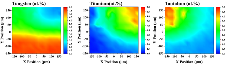 Figure 4. Quantitative alloy composition maps of the investigated ternary junction region.
Some general features are also notable within the mechanical property maps. Vertical striations within the Hardness and H/Er ratio maps are attributed to residual subsurface grinding damage from surface preparation, as they are not visible in the reduced modulus or BSE micrographs. Higher hardness is observed in both the bottom side, close to the base alloy, and the upper left side, close to alloy 5Ta4W. Lower hardness is observed in the upper right side near alloy 10Ti2W. It is interesting to note that the hardness varies from 5.3 ~ 5.8 GPa within the Base region, even though chemical concentration was approximately constant, as shown in Figure 4. This phenomenon is attributed to the variation in grain orientation, due to the reduced modulus variation, and the grain boundaries can be distinctly observed in the property maps (Figure 3).
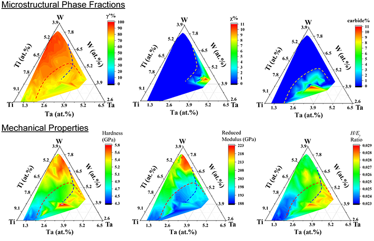 Figure 5. Ternary phase and mechanical property maps assembled from Correlative Mechanical Microscopy of the superalloy triple junction with precipitation phase regions marked with dashed lines (χ phase in blue, carbides in red).
In the upper left region, near alloy 5Ta4W, the hardness maps revealed three distinct phases: χ phase with a higher hardness of 6.3 ~ 6.7 GPa, γ+γ′ two-phase region with hardness of 5.0 ~ 5.2 GPa, and carbide phases with very high hardness of above 10 GPa. These are also noted in the BSE micrograph. The reduced modulus maps display the orientation variation within the base alloy, as well as the variation across the vertical interface between the base alloy and the 5Ta4W and 10Ti2W variants. A local depletion in reduced modulus is also clearly notable near the carbide phases.
The quantitative variation in composition over the diffusion ternary junction determined by compositional analysis is presented in Figure 4. As the quantity of Al, Co, and Ni varied little within the investigated region (~/< 1 %), it is not discussed further here. However, significant compositional gradients of W, Ti, and Ta are observed between the bottom, upper right, and left corners of the region. The alloying element concentrations smoothly varied from approximately 2.0 to 7.6 at. % W, 4.1 to 8.6 at. % Ti, and 0.6 to 4.6 at. % Ta, respectively. This is in reasonable agreement with the pre-designed initial alloys. This approximately spans a ~5% compositional space for three elements with 0.1% resolution, (see Section 2.1) which spans 1,326 alloy combinations!
Discussion
Correlation/Data Registration
To determine the correlation between measured mechanical properties and compositional variations, matching sample volumes are required to pair the datasets. However, compositional maps (Figure 4) were acquired an “alloy” scale for design purposes, whereas the property maps (Figure 3) acquired using high-speed nanoindentation were performed at the microstructural scale to determine single-phase properties. In order to obtain the average mechanical properties at the alloy scale, which is more meaningful for compositional design, high-speed nanoindentation maps were locally averaged to achieve a matching sampling grid to the compositional data.
Mechanical property maps of the Base-10Ti2W-5Ta4W triple-junction (Figure 3) were divided into a point matrix with a step size of 25 μm, and the data within a rectangle range of ±10 µm for each point was averaged to represent the mechanical properties of the alloy at that point. Microstructural phase fractions of γ′, χ, and carbide phases in each area with the same step size were quantitatively analyzed using Image-Pro software. Using these correlated results, the quantitative relationships between ternary composition, microstructural phase fractions, and mechanical properties were determined - Figure 5.
Microstructural Trends
In terms of superalloy microstructural phases, the most important is the γ′ area fraction. Figure 5 indicates that W plays the most critical role for maintaining a higher γ′ area fraction, followed by Ta and Ti. This suggests that W is stronger at stabilizing γ′ phase than Ta and Ti in the current CoNi-base alloys. Precipitation phase regions are marked in Figure 5 with dashed lines: χ phase in blue, carbides in red.
χ, μ, and β phases are referred to as secondary, detrimental phases due to their negative influence on the mechanical properties of Co-base superalloys [14, 15]. Their irregular morphology and mismatched modulus cause stress concentrations within the matrix. Figure 5 illustrates that Ta exhibits a strong correlation with the precipitation of χ phase, more so than that of W and Ti.
The precipitation of carbides in these superalloy combinations is related to high contents of Ta and Ti (Figure 5) but is less affected by W. Ti and Ta are the primary carbide formers in superalloys [1], so this is consistent. The carbide precipitates in the current triple junction have a block morphology (Figure 3) and are enriched with Ta and Ti, indicating that they are MC-type carbides [1].
Mechanical Property Trends
With the compositional trends in microstructural phases identified, the trends in mechanical properties as a function of ternary composition within each phase region can now be determined. The high-throughput experimental results in Figure 5 show that increasing W and Ta contents significantly improve the hardness of the alloy within the γ′ phase region. The effect of W is greater than that of Ta, while Ti has the weakest effect among the three elements. Generally, there is a strong positive correlation between alloy strength and hardness [16]. Therefore, W provides a greater strengthening effect than Ta and Ti in these CoNi-base superalloys.
Strengthening effects in superalloys arise primarily from two contributions: solid-solution strengthening and precipitation strengthening [1]. In the current CoNi-base alloys, the precipitation strengthening effect is dominant as the content of γ′ precipitate exceeds 60%. This implies the main mechanism of plastic deformation is dislocation cutting of γ′ phase. Therefore, the alloy’s strength is related to the formation energy of antiphase domain boundary (EAPB) of γ′ [1]. First-principles studies [16] show that the predicted EAPB of L12-Co3(Al, W) is significantly higher than that of L12-Co3(Al, Ta) and L12-Co3(Al, Ti). This suggests that enriched W content would produce greater strengthening effects in the γ′ phase than Ta or Ti content in Co-base superalloys. This is in good agreement with the current results.
In Ni-base superalloys, all three of the elements considered here (W, Ta, and Ti) produced significant contributions to solid solution strengthening of the γ matrix and to precipitation strengthening of γ′ phase, with Ta reportedly producing greater strengthening effects than W and Ti [17]. We observe that this is not the case in CoNi-base superalloys, highlighting the necessity for high-throughput investigations for development of novel superalloys.
Elastic properties are one of the fundamental parameters of structural materials. Within single grains of materials, indentation can only measure the reduced modulus, which generally exhibits a positive correlation with the elastic modulus [18], as the local Poisson’s ratio is unknown. In polycrystalline materials or grains of known orientation (and Poisson’s ratio), it is possible to determine the elastic modulus from the reduced modulus [11, 19]. However, as this work investigates a range of novel compositions, only the reduced modulus is discussed here. The high-throughput results show that the alloy compositions enriched in W have a higher reduced modulus, greater than that of Ti or Ta - Figure 5. This seems reasonable as the elastic modulus of pure W is higher than that of Ti and Ta [20]. Higher elastic modulus is desirable in these structural materials, as it indicates a higher strain-hardening coefficient. In addition, a high elastic modulus is beneficial to reducing the steady creep rate at high temperature, which is one of important effects of solution strengthening [1]. Therefore, a moderate content of W appears to be beneficial for strengthening CoNi-base superalloys.
The H/Er ratio, or plasticity index, is generally positively correlated with the wear resistance of alloys [21]. Figure 5 shows the influence of compositional variations of Ta, Ti, and W content on H/Er ratio. Alloy compositions in Ti-rich region display lower H/Er ratios, while the Ta-rich region exhibits higher values. Previous research indicates that the H/Er ratio of different phases within the same alloy system often possess a large gap [19]. Therefore, the high H/Er ratio in Ta-rich alloys is attributed to the precipitation of the χ phase. Furthermore, both the W-rich region and Ti-rich region are γ/γ′ two-phase regions, suggesting that the variation of H/Er ratio in these regions is due to the variations of W and Ti content. This implies the substitution of W for Ti increases the H/Er ratio of CoNi-base alloys and would be beneficial for improving their wear resistance.
Conclusions
In this application note, correlative mechanical microscopy was applied in a high-throughput combinatorial investigation to determine the alloying effects of W, Ti and Ta on the microstructural and mechanical properties of Co-20Ni-7Al-8W-4Ti-1Ta superalloys. A combinatorial library was generated using a carefully-designed diffusion-multiple to provide a large compositional space for investigation. A combination of electron microscopy image analysis, quantitative compositional analysis, and high-speed nanoindentation was performed to determine quantitative relationships between microstructure, alloy composition, and mechanical properties using correlated datasets. A large compositional space were considered, i.e., W: 2~8 at.%, Ti: 4~10 at.%, Ta: 1~5 at.%. This approximately spans a ~5% compositional space for three elements with 0.1% resolution, comprising 1,326 alloy combinations within a single experiment!
In terms of microstructure, W plays the most critical role for achieving a high γ′ area fraction, followed by Ta and Ti. This suggests that W is stronger than Ta and Ti in stabilizing γ′ phase in the current CoNi-base alloys. Therefore, a moderate content of W is necessary for this class of alloys. Ta strongly promotes the precipitation of χ phase with a threshold of ~3.6 at.%. Although W is a χ phase former element, it does not promote the precipitation of χ phase at contents below 8 at.%. In addition, high contents of Ta and Ti lead to formation of MC carbide phases.
In terms of mechanical properties, increasing W and Ta contents significantly improve the hardness of the alloy. To this end, the effect of W is stronger than that of Ta, while Ti has the weakest effect among these three elements. On the other hand, the W-rich alloys exhibit significantly higher elastic modulus than that of Ta-rich or Ti-rich alloys.
These high-throughput results allowed the design of an optimized compositional range to achieve a balance of properties with low density, high γʹ area fraction, and alloy strength with W, Ti and Ta contents ranged as followed, 4.3~4.9, 5.7~6.5, 1.8~2.1, at.%.
Correlated microstructure, composition, and mechanical properties datasets obtained on combinatorial samples using the methods described in this study provide significant insights into the complex influence of alloying elements within multi-component alloys. This demonstrates the potential of correlative mechanical microscopy for the high-throughput investigations of complex alloys.
Acknowledgements
The authors would like to thank his collaborators at Xiangtan University and the State Key Laboratory for Advanced Metals and Materials, University of Science and Technology Beijing in China. Full details on this work are available in a publication in Materials Science and Engineering: A.
W. Li, J.M. Wheeler, H. Han, L. Li, Q. Feng. High-throughput investigation of the alloying effects of W, Ti, and Ta on the micro-structural stability and mechanical properties of CoNi-base superalloys, Materials Science and Engineering: A (2025) 147857. https://doi.org/10.1016/j.msea.2025.147857
References
- J. Guo, Materials science and engineering for superalloys,Science Press, Beijing, 2008.
- R.C. Reed, The superalloys: fundamentals and applications,Cambridge University Press, Cambridge, 2006.
- A. Suzuki, H. Inui, T.M. Pollock, Ann. Rev. Mater. Res., 45 (2015)345-368.
- X. Zhuang, S. Antonov, W. Li, S. Lu, L. Li, Q. Feng, Acta Mater.,243 (2022) 118525.
- M. Zou, W. Li, L. Li, J.-C. Zhao, Q. Feng, in: S. Tin, M. Hardy,J.Clews, J. Cormier, Q. Feng, J. Marcin, C. O’Brien, A. Suzuki(Eds.) Superalloys 2020: Proceedings of the 14th IntenationalSymposium of Superalloys, Springer International Publishing,Champion, PA, 2020, pp. 937-947.
- S. Lu, M. Zou, X. Zhang, S. Antonov, W. Li, L. Li, Q. Feng,Advanced Engineering Materials, 25 (2023) 220125.
- X. Zhuang, S. Antonov, L. Li, Q. Feng, Metall. Mater. Trans. A,(2023).
- W.C. Xiao, S.F. Liu, Y.L. Zhao, J.J. Kai, X.J. Liu, T. Yang, Journal ofMaterials Research and Technology, 23 (2023) 2343-2350.
- S. Neumeier, L.P. Freund, M. Göken, Scr. Mater., 109 (2015)104-107.
- J.C. Zhao, X. Zheng, D.G. Cahill, Materials Today, 8 (2005)28-37.
- J.M. Wheeler, B. Gan, R. Spolenak, Small Methods, 6 (2022)2101084.
- W. Li, L. Li, S. Antonov, C. Wei, J.-C. Zhao, Q. Feng, J. AlloysCompd., 881 (2021) 160618.
- W. Li, L. Li, C. Wei, J.-C. Zhao, Q. Feng, J. Mater. Sci. Technol.,80 (2021) 139-149.
- M. Wen, Y. Sun, J. Yu, Y. Yang, Y. Zhou, X. Sun, J. AlloysCompd., 835 (2020) 155337.
- X. Zhou, H. Fu, F. Xue, Y. Zhang, J. Xie, Scr. Mater., 181 (2020)30-34.
- A. Mohammadzadeh, A. Heidarzadeh, H. Becker, J.V. Robles,A.Meza, M. Avella, M.A. Monclús, D. Tourret, J.M. Torralba, Journalof Alloys and Compounds, 965 (2023) 171380.
- S. Antonov, M. Detrois, D. Isheim, D. Seidman, R.C. Helmink,R.L. Goetz, E. Sun, S. Tin, Mater. Des., 86 (2015) 649-655.
- Y.W. Bao, W. Wang, Y.C. Zhou, Acta Mater., 52 (2004) 5397-5404.
- J.M. Wheeler, Journal of Materials Research, 36 (2021) 94-104.
- S.L. Shang, A. Saengdeejing, Z.G. Mei, D.E. Kim, H. Zhang, S.Ganeshan, Y. Wang, Z.K. Liu, Comput. Mater. Sci., 48 (2010) 813-826.
- B.D. Beake, Surface and Coatings Technology, 442 (2022)128272.

