Mechanical microscopy often provides mechanical images which clearly show grain structure and/or different phases within the microstructure. These can often be blindly deconvoluted using cluster analysis if they are sufficiently mechanically distinct, but additional crystallographic information is needed in order to determine structure-properties relationships for the study of anisotropy or grain boundary behavior. This can be achieved using correlated electron back-scattered diffraction (EBSD) mapping to provide structural information. Using displacement-controlled indentations allowed consistent sampling from both mechanical and EDX sampled volumes, as well as reducing variation in surface damage by the indentations by restricting the deformed sub-surface volume. This demonstrates the potential of this correlative approach for studying structure-property relationships and offers a new tool for the study of plastic and elastic anisotropy.
Introduction
A core theme of materials science is the relationship between microstructure and mechanical properties. Characterization techniques are what allows the connection between these aspects of materials, and mechanical microscopy offers a powerful new way to simultaneously measure microstructure and mechanical properties together. However, nanoindentation alone does not provide structural information on the material: crystal structure and orientation. To acquire this information, a popular method is to use electron back-scattered diffraction (EBSD) using a special detector inside a scanning electron microscopy (SEM). By combining nanoindentation and EBSD mapping on polycrystalline microstructures, correlative mechanical microscopy can provide information on both the plastic and elastic anisotropy of materials.
The combination of nanoindentation and analytical electron microscopy is uniquely well-suited for such correlative investigations. Their mutual micrometric length scale allows them to locally interrogate with high spatial resolution. However, for a technique to be truly correlative, all measurements need to be mutually coincident, so that the crystal phase and orientation and mechanical properties of each location are known. Earlier applications of correlative microscopy with indentation have been limited to determining orientation relationships to mechanical behavior with manually-selected locations. This was employed by Vlassak and Nix [1] in their investigation the ability of nanoindentation to measure elastic anisotropy in materials. This was done by performing indentations in selected grains of desired orientation after EBSD mapping.
By using nanoindentation mapping in combination with EBSD mapping, structure and mechanical properties data can be acquired in a more high-throughput manner. This was first demonstrated on Titanium alloys by Magazzeni et al. [2], which successfully allowed hardness trends with orientation to be measured. However, the nanoindentation mapping technique employed was limited to monotonic load-unloading testing, which restricted the precision of the contact stiffness measurement and prevented clear trends in modulus vs orientation from being determined.
In this application note, nanoindentation and orientation mapping are used to perform correlative mechanical microscopy on a polycrystalline 316L stainless steel sample. An indentation technique employing continuous stiffness measurement (CSM) is used, providing sufficient precision to determine reduced modulus as a function of orientation. Details of the approach are described, particularly the system concerns, and the ability of the correlative approach to identify grains and trends in both elastic and plastic anisotropy is demonstrated and discussed.
Experimental Considerations
For a system to perform this application, two factors are important to remember: Displacement control and Sensitivity. To perform correlative mechanical microscopy, the sampled volumes measured by both techniques need to be similarly and regularly sized. For nanoindentation, this means that testing should be performed under displacement control, so that every indentation is made to the same maximum depth regardless of that phase’s or orientation’s properties. The measurement sensitivity is extremely important, as orientation variations may only produce slight mechanical changes.
Displacement Control
Displacement-controlled indentation mapping is highly preferable for correlative applications. In load control, the load must be carefully chosen to ensure that the spacing is proportional to the indentation produced in the softest phase in the map. Otherwise, indentations in the soft region will overlap with its neighbors. This means for indentations maps performed in load control, a significant disparity in indentations depths and spacings can be expected for maps over dissimilar phases.
In displacement control, indentations are all performed to the same maximum depth, ensuring similar indentation sizes and regular with minor variations from differences in elastic recovery. This is important for correlative measurements, so that every mechanical and analytical measurement is taken from the same volume of material.
System Sensitivity
High speed, regular maps of indentations are not useful unless the measurement sensitivity is high enough to resolve the variations within the mapped region. The measurement sensitivity is a function of several parameters: force and displacement noise floors, system dynamics, repeatability.
The primary influence on system’s measurement sensitivity is its noise floor in both force and displacement. For performing nanoindentation maps, tolerances in measurement noise must be very tight, particularly for identifying the contact point and during CSM measurements.
Continuous stiffness measurement during nanoindentation allows the acquisition of many stiffness datapoints to be acquired as a function of penetration depth during a single indentation. This is how hardness and reduced modulus can be measured as a function of depth during indentation. To prevent fatigue of the near surface [3] and accurately capture the indentation size effects these oscillations should ideally be small relative to the indentation force and depth during the oscillation. Thus, it is important that the initial oscillation amplitude is kept sub-nanometer, so that the force amplitude of the oscillation is also kept to a small fraction (in this case ~15%) of the total load.
Experimental Procedures
Samples of austenitic 316L stainless steel were acquired in the as-rolled sheet condition. To obtain an equiaxed, annealed microstructure, these were sectioned into 2×10×10 mm pieces and heat treated in a tube furnace (HTRH 40-100/16, Carbolite Gero GmbH & Co. KG, Germany) under in forming gas (5% H2–Ar of 99.95% purity) atmosphere at 1000 °C for 3 hours. The samples were then metallographically prepared in cross-section by embedding in Bakelite (LaborPress-3, Struers GmbH, Switzerland), followed by grinding and polishing (RotoPol-21, Struers GmbH, Switzerland) with SiC 300, 600, 1200, 2400, 4000; diamond suspension 3 μm, 1 μm, 0.25 μm; Al2O3 suspension 50 nm).
Nanoindentation maps of 200×150 indents were performed on each sample using an i04 Femto-Indenter with a diamond Berkovich indenter on a FT-S20,000 sensor. Each indentation was performed using a CSM [4] in displacement control. The indentations were each performed in ~1 s with an oscillation frequency of 150 Hz and an amplitude that increased from 0.5 to 2.5 nm with depth. The total time for each indentation including repositioning was ~2.5 seconds.
Each indentation was performed to a specified depth of 190 nm, so that a spacing of 2 µm between indentations could be used while still ensuring an indentation depth/spacing ratio of 10 was maintained [3]. This avoids any significant interaction between neighboring indents. Hardness and reduced modulus were measured as a function of depth for each location, and representative values for each were taken by averaging values from depths >150 nm to minimize the influence of indentation size effects for hardness values and >100 nm for modulus values.
EBSD Characterization
To obtain the size and crystallographic orientation distributions of the grains within the microstructure, EBSD measurements were performed using a Hitachi SU70 SEM equipped with a field-emission gun operated at 20 kV with a HKL Nordlys EBSD camera. EBSD measurements were performed with a step size of 1 μm and using a 4×4 binning and averaging of 2 frames. Noise reduction was performed using 5 nearest neighbors. Electron micrographs were taken of the test region with a Zeiss EVO 25 SEM at 10 kV using a HD Backscattered Electron Detector (BSE).
Due to the 70° tilt required for EBSD, some misalignment or distortion of the region of interest is likely. To correct for this, correlation between the EBSD and indentation maps was performed using an affine transformation of the matrix coordinates to produce a 1:1 overlay of the two datasets similar to in [2]. This provides paired datasets with mechanical properties and orientation vectors for each indentation. Software tools for this type of correlation are available.
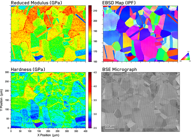 Figure 1. Indentation property maps of the annealed 316L stainless steel sample with the corresponding orientation map from EBSD and a BSE micrograph of the indentation grid.
Results
The results of correlative nanoindentation and EBSD mapping are shown in Figure 1. Excellent visual correlation is observed between the reduced modulus, Er, and EBSD maps in both morphology and scaling, as well as with the morphology of the BSE micrograph of the region. Nearly all grains in the EBSD map can be clearly distinguished in the reduced modulus map with only a few adjacent grains of similar orientations being difficult to separate.
By eye, several different types of grains show prominence within the EBSD map. Dark blue, [111]-oriented grains appear to be the most common, followed by magenta, [112]-oriented grains. These generally correspond to red, high modulus and green, intermediate modulus grains within the reduced modulus plot. There is a relatively small number of [100]-oriented, red grains in the EBSD map, and these correspond to low modulus, blue grains in the reduced modulus map.
The hardness map and BSE micrograph show similar morphology to the reduced modulus and EBSD maps, but the intensities in these maps do not as directly correspond to the orientations or moduli of the grains in all cases. The grains which are near the [100]-orientation do appear to have the lowest hardness, H, and several of the [111]-oriented grains appear to have higher hardness. However, exceptions to this trend are easily observed. The hardness map also shows features which are not observable in any of the other three contrast mechanisms. Several grain boundaries show local increases in hardness which ‘highlights’ the boundaries. This could be attributed to two different mechanisms: grain boundary-dislocation interactions [5-7] or elemental segregation at grain boundaries [8]. While it is likely that this technique could be used to study both of these mechanisms, in this case, it is most likely from the magnitude of the hardening that it is due to solute segregation at the grain boundaries [8]. There is no evidence of larger secondary precipitate phases at the boundaries in the BSE micrograph, so any such precipitates are presumed to be nanoscale.
Discussion
Correlative techniques are very important for data analysis to identify trends between the crystal orientation and/or phase and mechanical techniques, as analysis of one technique alone may be insufficient for data segmentation or deconvolution of overlapping clusters [9].
As hardness and elastic modulus are interrelated properties, 2D histogram plots are utilized to display the statistical distributions of the obtained H and E values over the entire mapped region simultaneously. As demonstrated in previous work [9-12], this type of plot shows the number of indentations fitting within a fixed bin of H and E values such that phases appear as clusters or peaks. The color of each pixel represents the number of indentations that are included within a range of H and E, which is defined as a 2D bin size. Values of only 1 indent are shown in light gray to minimize the visual impact of outliers, and higher indentation numbers are shown with a shaded gradient from darker red tones to yellow-white peaks at the highest values in each histogram.
These are therefore arbitrary units, depending on the number of total indentations performed. In this study, 30,000 indentations were performed on the 316L stainless steel sample, so typical peak values for the histograms are between 30-50 indentations. These figures offer a simple visual method to evaluate ‘hot spots’ in the indentation property space which statistically correspond to individual phases. As shown in previous work [10], these ‘peaks’ in the 2D histograms often take the form of elliptical, normal distributions which are elongated along the direction of the H/E ratio.
Using the correlated EBSD data, the data can also be represented using a 2D scatter with the color indicating the crystal orientation, similar to previous correlative EDX studies [13] which indicated composition using color on a similar plot. This plot reveals the correlation between the peaks in the 2D histogram plot and the crystallographic orientation. As noted earlier in Figure 1, the majority of the region was composed of blue, [111]-oriented and magenta, [112]-oriented grains. This is can now be shown to correlate with the two main peaks observed in the 2D histogram plot. This shows how the mechanical properties relate to the texture of the microstructure. Smaller clusters can also be seen for the few small red, [100] grains in the lower left corner of lowest hardness and modulus and for the higher hardness, solute-strengthened grain boundaries between the [112] and [111] grains.
This plot of indentation properties and orientation represents a unique way of simultaneously showing both elastic and plastic anisotropy relationships with crystallographic orientation in a material or a fingerprint of its deformation behavior. The shape of the distribution depends on the relationship between elastic and plastic anisotropy, while the coloring indicates the relationship of this anisotropy to the crystallographic orientation. In this case, as the sampled region did not possess a completely random texture (all orientations evenly distributed), the fingerprint is not complete. However, several general trends can be observed. The distribution is mostly oblong, oriented along a single H/E ratio, as seen previously in FCC materials [10]. However, this current work reveals that the hardness and modulus increase along this H/E axis smoothly as a function of crystallographic orientation with the minimum at the [100] and a maximum at [111] orientations. [112] and [101] orientations appear to give intermediate values, though some values for [112] and [111] orientations are harder than the main cluster due to the elemental segregation at the grain boundaries noted earlier.
Despite being Austenitic with an FCC crystal structure, 316L stainless steel is still elastically anisotropic [14]. Its elastic modulus values range from 101.6 GPa for the soft [100] orientation to 285.1 GPa for the hard [111] orientation. However, this is not the range of modulus that we measure with indentation. Instead, due to the complex stress state beneath the indenter tip, a reduced spread in modulus is measured. Through extensive finite element modelling, Vlassak and Nix [1] worked out a relationship for this effect. Applying their equation with our elastic tensor values for 316L Steel gives the following range of reduced modulus values: [100] orientation = 162.7 GPa and [111] orientation = 185.6 GPa. This is in good agreement with the range of values observed in the 2D histograms in Figure 2. The maximum observed modulus values are slightly higher than expected from Vlassak and Nix estimates, suggesting either that some spread exists in the data or that a small degree of pile-up is likely to have occurred around the indentations, elevating the apparent modulus.
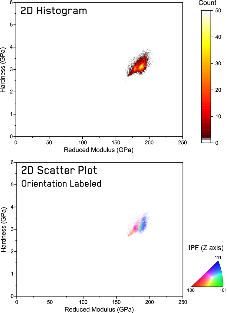 Figure 3. 2D histogram of indentation results from 316L stainless steel, and 2D scatter plot of results with IPF color labeling. This shows trends in hardness and reduced modulus with crystallographic orientation.
Conclusion
The application of correlative mechanical microscopy and EBSD for the investigation of crystal orientation and mechanical properties was successfully demonstrated on 316L stainless steel. Unlike EDX correlation, an affine transformation was necessary to align the indentation and EBSD maps. Using displacement-controlled indentations allowed consistent sampling from both mechanical and EBSD sampled volumes. In general, hardness and modulus of the grains were observed to scale with their orientation. However, some grain boundaries appeared harder than their surroundings, suggesting elemental segregation to the grain boundaries occurred during annealing. The additional structural information provided by EBSD revealed the influence of crystallographic texture on the indentation datasets, with histogram peaks corresponding to [112] and [111] orientations. General trends in the orientation dependence of the hardness and modulus, corresponding to variations in elastic and plastic anisotropy, were elucidated using an orientation-labeled 2D scatter plot. For FCC Austenite, the hardness and modulus were observed to smoothly increase with orientation as it rotated from a minimum at the [100] orientation to its maximum at the [111] orientation. The range of measured reduced moduli measured was found to be in good agreement with values calculated using Vlassak and Nix’s relations from the elastic tensor for 316L steel. This demonstrates the potential of correlated mechanical microscopy with EBSD for future investigations.
Acknowledgements
The author gratefully acknowledges the contributions of several groups who assisted in these measurements. Dr. Marius Wagner of Prof. Spolenak’s Laboratory for Nanometallurgy at ETH Zurich produced and metallographically prepared the sample of 316L steel. Dr. Indranil Basu of Prof. Loffler’s Laboratory of Metal Physics at ETH Zurich performed the EBSD characterization. EBSD and nanoindentation correlation was done by Sang-Hyeok Lee in the Department and Chair of Physical Metallurgy and Material Physics at RWTH in the group of Prof. Sandra Korte-Kerzel.
References
- J.J. Vlassak, W.D. Nix, J. Mech. Phys. Solids, 42 (1994) 1223-1245.
- C.M. Magazzeni, H.M. Gardner, I. Howe, P. Gopon, J.C. Waite, D. Rugg, D.E. Armstrong, A.J. Wilkinson, Journal of Materials Research, 36 (2021) 2235-2250.
- M.J. Cordill, M.S. Lund, J. Parker, C. Leighton, A.K. Nair, D. Farkas, N.R. Moody, W.W. Gerberich, International Journal of Plasticity, 25 (2009) 2045-2058.
- W.C. Oliver, G.M. Pharr, Journal of Materials Research, 7 (1992) 1564-1583.
- F. Javaid, H. Pouriayevali, K. Durst, Journal of Materials Research, 36 (2021) 2545-2557.
- S. Pathak, J. Michler, K. Wasmer, S.R. Kalidindi, J. Mater. Sci., 47 (2012) 815-823.
- J.S. Weaver, D.R. Jones, N. Li, N. Mara, S. Fensin, G.T. Gray III, Materials Science and Engineering: A, 737 (2018) 373-382.
- M. Tomozawa, Y. Miyahara, K. Kako, Materials Science and Engineering: A, 578 (2013) 167-173.
- H. Besharatloo, J.M. Wheeler, Journal of Materials Research, 36 (2021) 2198-2212.
- J.M. Wheeler, Journal of Materials Research, 36 (2021) 94-104.
- Y. Xiao, H. Besharatloo, B. Gan, X. Maeder, R. Spolenak, J.M. Wheeler, Journal of Alloys and Compounds, 822 (2020) 153536.
- K. Wieczerzak, J. Michler, J.M. Wheeler, S. Lech, R. Chulist, J.Czub, A. Hoser, N. Schell, P. Bała, Materials & Design, 188 (2020) 108438.
- J.M. Wheeler, B. Gan, R. Spolenak, Small Methods, 6 (2022) 2101084.
- H.M. Ledbetter, physica status solidi (a), 85 (1984) 89-96.

