Oxford Instruments will be showcasing our cutting-edge technologies. This includes our nanoindentation technology, Atomic Force Microscopy (AFM), confocal Raman microscopy, and electron microscopy detectors. We are proud to unveil exciting developments that are currently in the pipeline and offer live demonstrations of our latest innovations. Visit our booth to experience firsthand the advancements we are making in these fields.
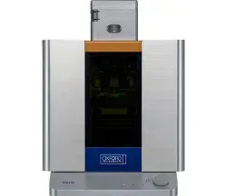
Vero S is the standard ambient configuration of the next-generation Vero AFMs, which precisely and accurately measure true tip displacement using Quadrature Phase Differential Interferometry (QPDI).
Learn more about the Vero S
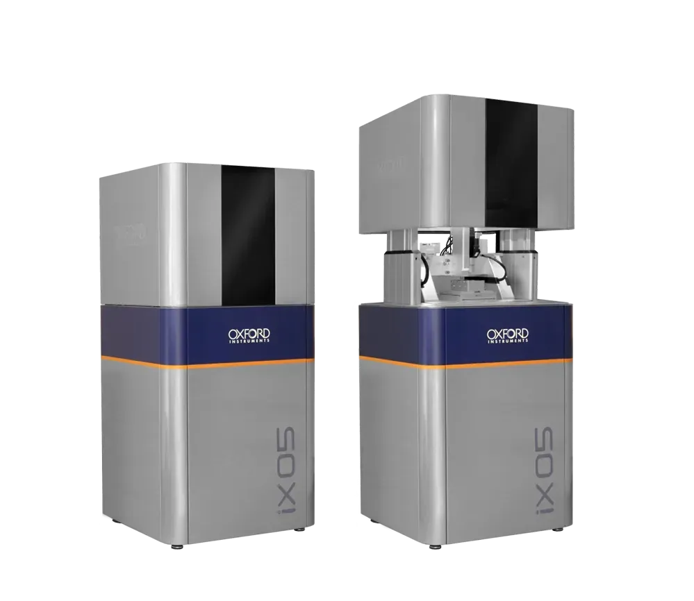
iX05 Operando Nanoindenter
The iX05 is a high-performance operando nanoindenter engineered to measure local mechanical properties under real-world conditions—including high/low temperatures, high strain rates, and liquid environments. Unlike traditional systems limited to lab settings, the iX05 enables testing in environments that reflect actual material applications. Powered by FemtoTools’ MEMS-based technology and fast control electronics, it delivers unmatched resolution, speed, and environmental control for advanced materials research.
Learn more about Nanoindentation
witec360 Raman Microscope
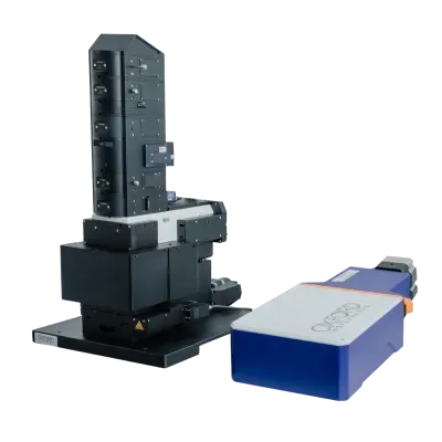
The Oxford Instruments witec360 is the new benchmark for Raman imaging and correlative microscopy systems, designed to meet the growing demands of academic and industrial researchers for comprehensive analysis at the nanoscale.
Learn more about the witec360
Symmetry S4
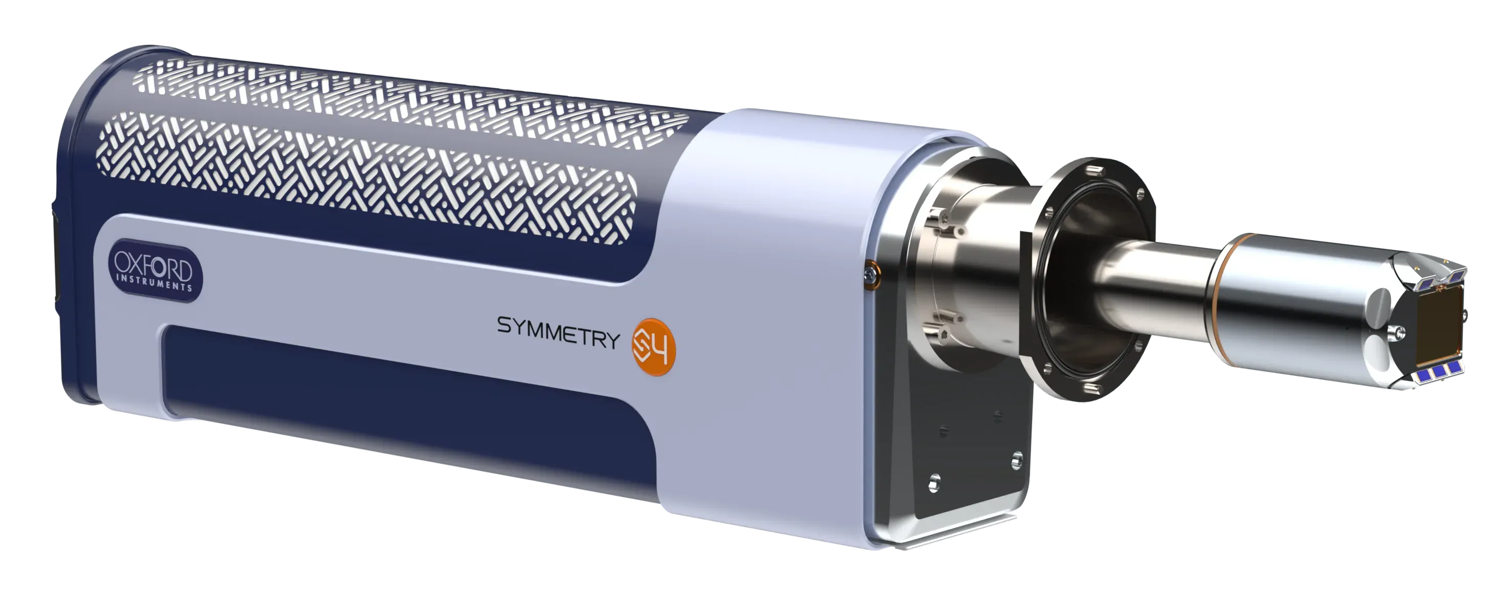
For years, real-time pattern matching has been viewed as the next advancement in microscopy analysis. With Symmetry S4, that capability is now available directly within your workflow.
Symmetry S4 identifies and matches diffraction patterns in real time, enabling immediate feedback as data is acquired. By combining automated pattern recognition with on-the-fly analysis, researchers can make informed decisions faster and gain deeper insight during every experiment.
More than a new software capability, Symmetry S4 represents a new approach to microscopy, moving beyond data collection to real-time interpretation and discovery.
Learn more about Symmetry S4
Join us for a one-on-one or group demo for AFM, Nanoindentation, or Raman.
We will be featuring a live Vero AFM system, a remote iX05 nanoindenter, and a remote witec360 confocal Raman microscope at booth 608.
AFM Group Demos:
Tuesday
3:00 p.m.: How to Achieve Atomic Lattice Resolution
5:15 p.m.: Beyond Automation: Connecting AFM to AI
Wednesday
9:00 a.m.: Ferroelectrics Imaging with Interferometric Detection
10:00 a.m.: Beyond Automation: Connecting AFM to AI
2:00 p.m.: Moiré Imaging of Stacked 2D Materials
Thursday
9:30 a.m.: Beyond Automation: Connecting AFM to AI
10:15 a.m.: Ferroelectrics Imaging with Interferometric Detection
Learn how high-resolution Torsional Force Mode imaging can reveal moiré patterns and nanoscale structural features in stacked 2D materials.
Explore nanoscale ferroelectric and piezoelectric properties with PFM, combining AFM topography with localized electromechanical measurements.
Experience how easy it is to achieve atomic lattice resolution to characterize defects in 2D materials that affect their device performance
AFM API Discussions with Asylum Research Experts to explore how APIs can connect AFM measurements to AI-driven decisions and scientific discovery.
Learn how MEMS-based nanoindentation enables large-area mechanical property mapping, revealing local variations in mechanical properties across complex materials and microstructures. Combined with EBSD and EDS datasets, this approach uncovers the influence of composition, crystallography, and microstructure on local mechanical behavior.
Learn how Raman, PL, and SHG imaging reveal the structure and optoelectronic properties of 2D materials.
As interest in 2D-material-based devices continues to grow, understanding atomic defects has become critical for optimizing performance. This tutorial series highlights AFM-based approaches for the routine detection and characterization of atomic-scale defects in TMDs and other 2D materials, combining practical measurement strategies with representative research applications.
Agenda
Learn More HereThursday, November 12: CAFM of atomic defects in TMDs
Matthew Rosenberger, Notre Dame
Thursday, December 10: LFM of atomic defects in 2D materials
Matthew Rosenberger, Notre Dame
Wednesday, January 20: CAFM imaging and electronic spectroscopy of atomic defects in 2D materials
Mehmet Baykara, University of California, Merced
Thursday, February 11: Autonomous defects detection & back-contact free CAFM
Umberto Celano, Arizona State University
Thursday, February 25: Higher eigenmode imaging of defects
Nikolai Severin, Humboldt University of Berlin
Thursday, March 11: Title to be determined
Jairo Valasco, University of California, Santa Cruz
Thursday, March 25: Understanding the physical mechanism behind atomic resolution imaging in conductive atomic force microscopy in air
Mario Lanza, National University of Singapore
Thursday, April 8: CAFM of defects in hBN
Matthew Rosenberger, Notre Dame