Industry Challenges
Production teams must rapidly identify defect root causes, reduce variability, improve reliability, and increase throughput while meeting demanding quality and yield targets.
 Part of the Oxford Instruments Group


From Innovation to Scalable Manufacturing: From academic research to industrial production, explore resources to advance your semiconductor research, refine your processes and prepare for manufacturing at scale.

Complete the form to speak with one of our specialists about your semiconductor application field.
Request an Expert ConsultationA guide to Oxford Instruments’ semiconductor solutions for R&D and manufacturing and production.
BrochureThe latest webinar on how integrated processing and characterization workflows for optimised semiconductor development.
Watch the webinarNew materials such as silicon carbide (SiC), gallium nitride (GaN), indium phosphide (InP), as well as advanced memory architectures, heterogeneous integration and advanced packaging technologies are driving performance gains across automotive, communications, power electronics, AI and quantum applications.
Whether in semiconductor manufacturing or research, understanding the relationships between material properties, process conditions, and device performance is essential for informed decision-making.
Production teams must rapidly identify defect root causes, reduce variability, improve reliability, and increase throughput while meeting demanding quality and yield targets.
Research laboratories require advanced characterisation methods to understand novel materials, investigate physical phenomena, and validate emerging technologies.
These complex semiconductor challenges rarely have a single cause. By combining structural, compositional, optical and mechanical data, multiple observations can be correlated to identify the mechanisms contributing to device failure or performance variation:
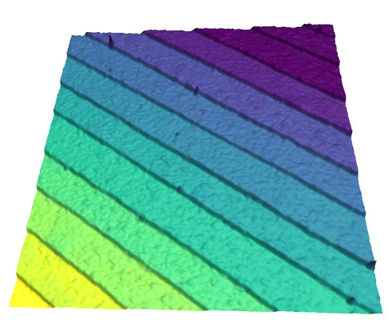
AFM supports defect analysis, semiconductor metrology and advanced process characterisation. Characterise with exceptional sensitivity:
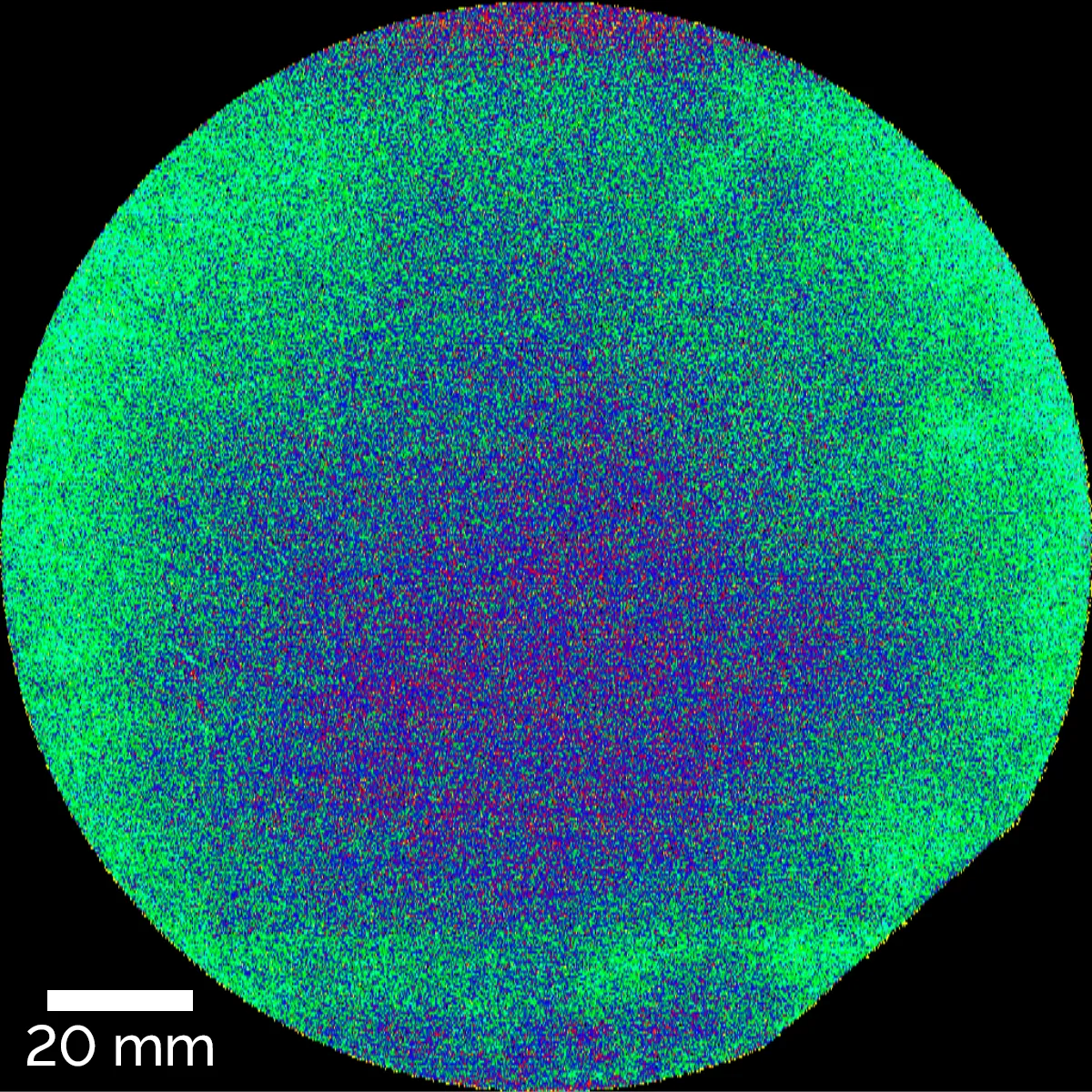
Raman spectroscopy enables wafer-level inspection, SiC characterisation and advanced materials research. Through non-destructive optical analysis you can understand:
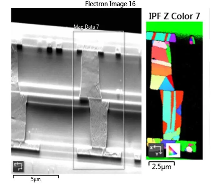
Reveal process issues, contamination sources and device failure mechanisms by correlating:
Nanoindentation can help understand reliability risks in multilayer semiconductor structures by evaluating:
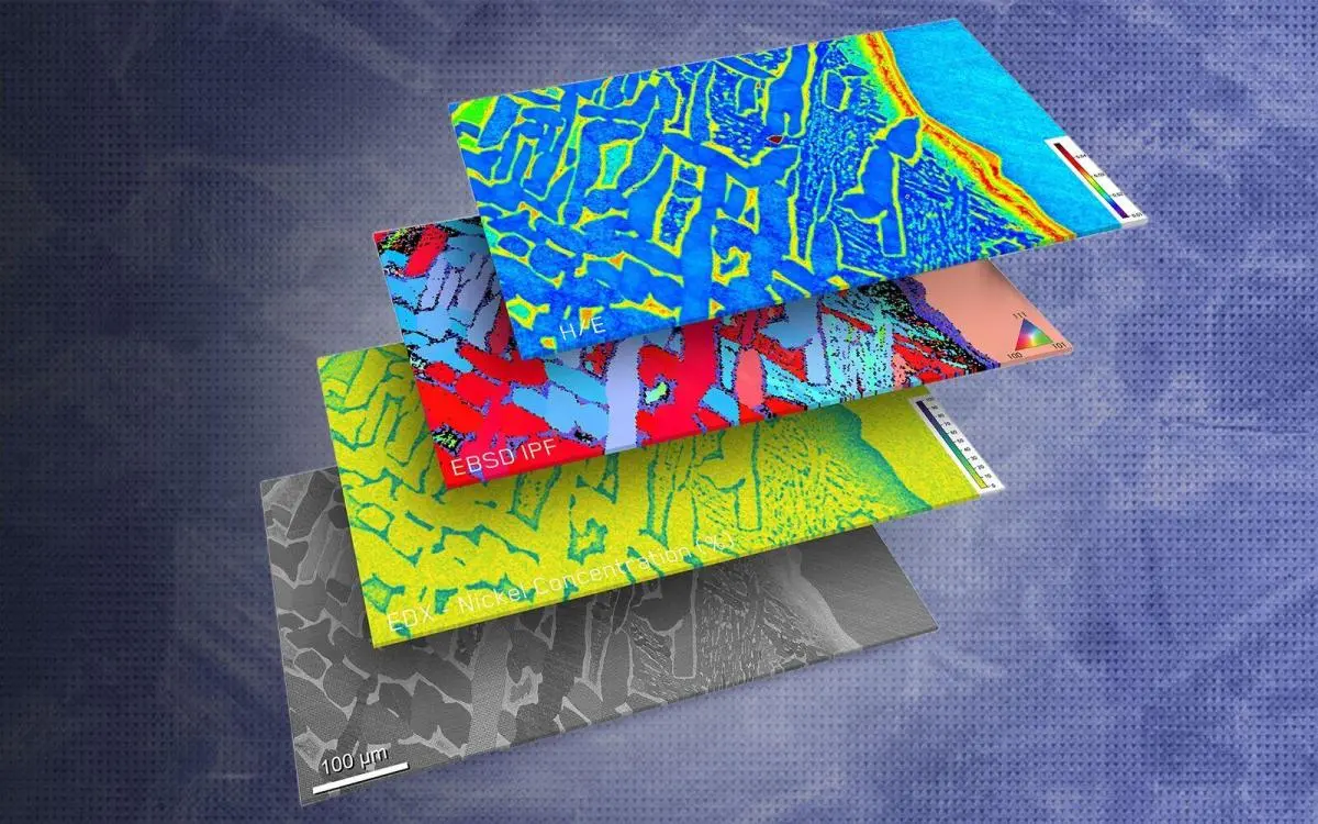
A power device manufacturer experiences an unexpected reduction in yield during qualification of a new SiC process. Initial electrical testing identifies underperforming devices, but does not reveal the cause. A correlative analysis approach can then be used to investigate the issue from multiple perspectives.
Raman spectroscopy is used to map residual stress within the device structure, electron microscopy with EDS provide information on microstructure and material composition, while AFM characterises surface morphology and process-induced defects. Nanoindentation provides insight into the mechanical properties and reliability of thin films and interfaces, helping identify potential failure mechanisms.
By correlating these complementary datasets, engineers can determine whether the observed performance variation is linked to material defects, process non-uniformity, contamination, or localised stress concentrations, enabling a more complete understanding of the underlying failure mechanism and informing subsequent process optimisation efforts.
Whether you're developing new materials, optimising manufacturing processes, improving reliability or investigating device failures, our specialists can help identify the most effective analytical approach for your application.
Request an Expert Consultation
© Oxford Instruments 2026