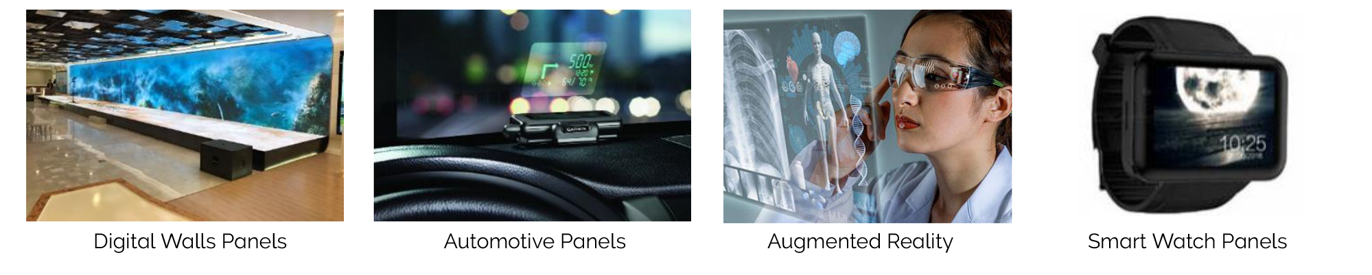
Augmented Reality
Augmented Reality, or AR, is a technology that allows users to visualize and interact with computer-generated objects layered on top of real-world environments.
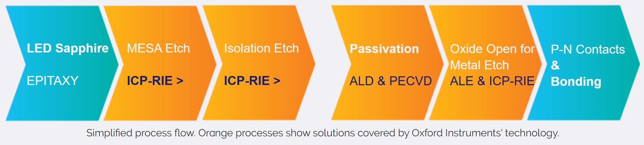
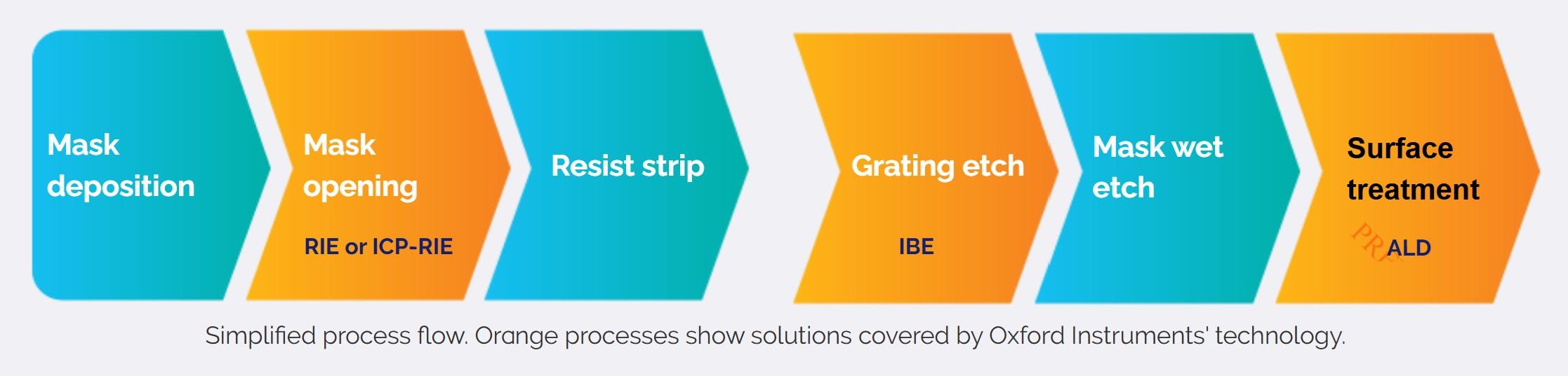
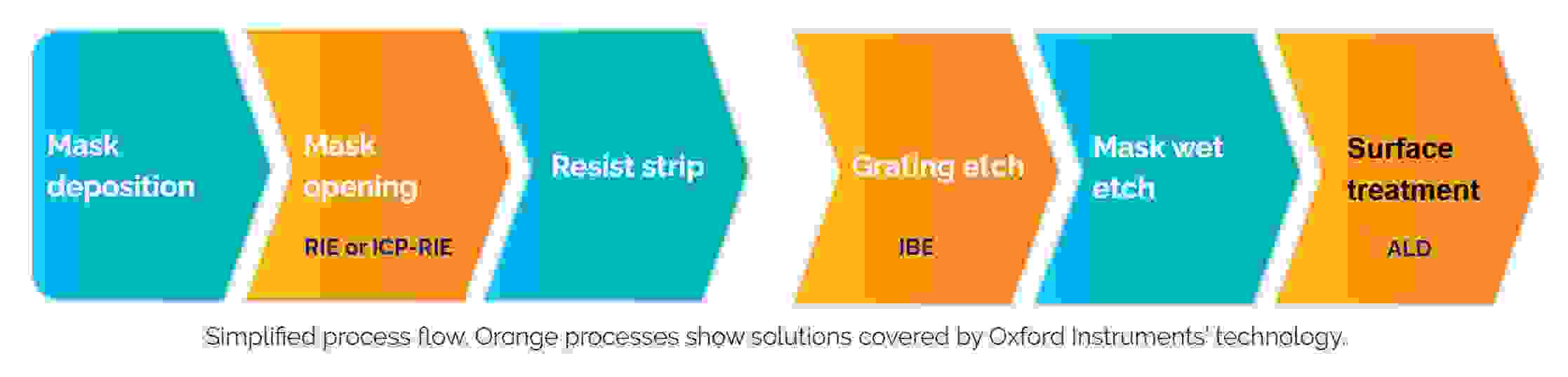
Our advanced plasma processing solutions – achieved with ICP Etching, RIE and Ion Beam Etching – can handle wafers up to 200mm in size for high-volume production of AR devices.
Cluster configuration options are available, using a field-proven, highly-reliable vacuum transfer robot for mask etching and AR coating modules.
ICP Etching
The PlasmaPro 100 process modules offer a 200mm platform with single wafer and multi-wafer batch capability. The process modules offer high throughput, high precision and excellent uniformity with clean smooth vertical profiles and etch surfaces. Our systems have a wide install base within high volume manufacturing (HVM), with well-developed process solutions.
- Excellent uniformity
- High-throughput, high-precision and low-damage processes for wafer sizes up to 200mm
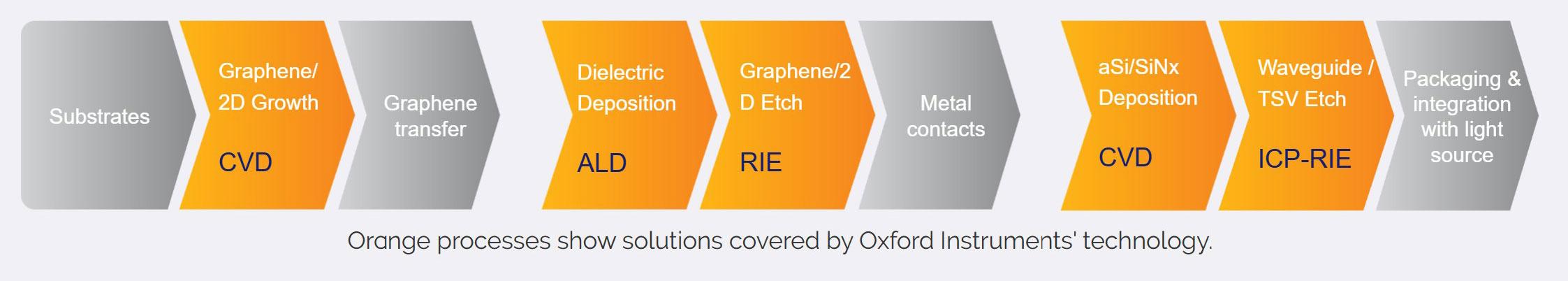
- Supporting a number of markets including, GaAs & InP laser optoelectronics, microLEDs & metalenses, SiC & GaN power electronics/RF and MEMS & sensors
Learn more here.
Ion Beam Etching (IBE)
Our Ionfab system for IBE has been configured for optimum uniformity on 200mm wafer size. Our proprietary ion beam technology and patent filed grid design allow us to produce standard 45° gratings with excellent precision. Our processing capability covers various materials such as Si and SiO2.
- Ion Beam Etching Modes
- Ion Beam Deposition Modes
Learn more here.
AR solutions with optimum optical performance
Related Resource
Related Solutions