The Raman Principle
The Raman effect is based on the inelastic scattering of light by the molecules of gaseous, liquid or solid
materials. The interaction of a molecule with photons causes vibrations of its chemical bonds, leading to specific
energy shifts in the scattered light. Thus, any given chemical compound produces a particular Raman spectrum when
excited and can be easily identified by this individual “fingerprint.”
Raman spectroscopy is a well-established, label-free and non-destructive method for analyzing the molecular
composition of a sample.
Raman Imaging
In Raman imaging, a confocal microscope is combined with a spectrometer and a Raman spectrum is recorded at every
image pixel. The resulting Raman image visualizes the distribution of the sample’s compounds. Due to the high
confocality of WITec Raman systems, volume scans and 3D images can also be generated.
No need for compromises
The Raman effect is extremely weak, so every Raman photon is important for imaging. Therefore WITec Raman imaging
systems combine an exceptionally sensitive confocal microscope with an ultra-high throughput spectrometer (UHTS).
Precise adjustment of all optical and mechanical elements guarantees the highest resolution, outstanding speed and
extraordinary sensitivity – simultaneously!
This optimization allows the detection of Raman signals of even weak Raman scatterers and extremely low material
concentrations or volumes with the lowest excitation energy levels. This is an unrivaled advantage of WITec systems.
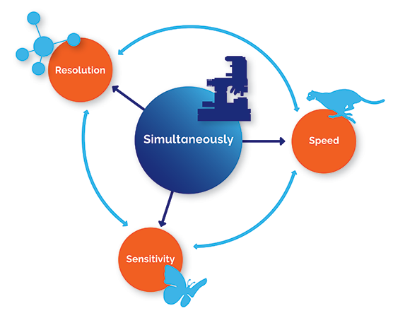
Resolution
Lateral resolution is physically limited to ~200 nm, depending on the wavelength of the incident light.
Sensitivity
A high confocality increases the signal-to-noise ratio by reducing the background. With the UHTS Series, WITec
developed lens-based, wavelength-optimized spectrometers with a spectral resolution down to 0.1 cm-1
relative wavenumbers.
Speed
The more sensitive a system is, the shorter the acquisition time for a single spectrum. WITec’s Ultrafast Raman
Imaging reduces acquisition times for single Raman spectra down to well below 1 ms.
Investigating compound semiconductors
Semiconductors and the detailed understanding of their properties have revolutionized electronics in recent decades.
They are employed in large numbers in optoelectronic devices such as integrated circuits (transistors, MOSFETs), solar
cells and diodes (light-emitting diodes, laser diodes, etc.). The chemical composition and crystal structure of a
semiconductor are essential in determining their electronic features. Therefore, precise metrology tools are required
to evaluate their material characteristics.
Confocal Raman microscopy and correlated techniques including photoluminescence (PL) are ideally suited for the
characterization of semiconducting materials and devices. Confocal Raman imaging, a non-destructive method, can
reliably detect material defects and stress fields in the crystals, as well as structural and chemical alterations and
doping in devices. This is especially useful for tracking chemical manipulations in electronics fabrication,
including the production of wafers. Additional photoluminescence analyses can reveal alterations in the bandgaps of
semiconductors.
This application note provides an overview of correlative Raman imaging, PL and topographic analyses of compound
semiconductors. It demonstrates the use of the WITec alpha300 Semiconductor Edition Raman microscope (Fig.1) to obtain
a thorough understanding on the composition, properties and defects of entire wafers.
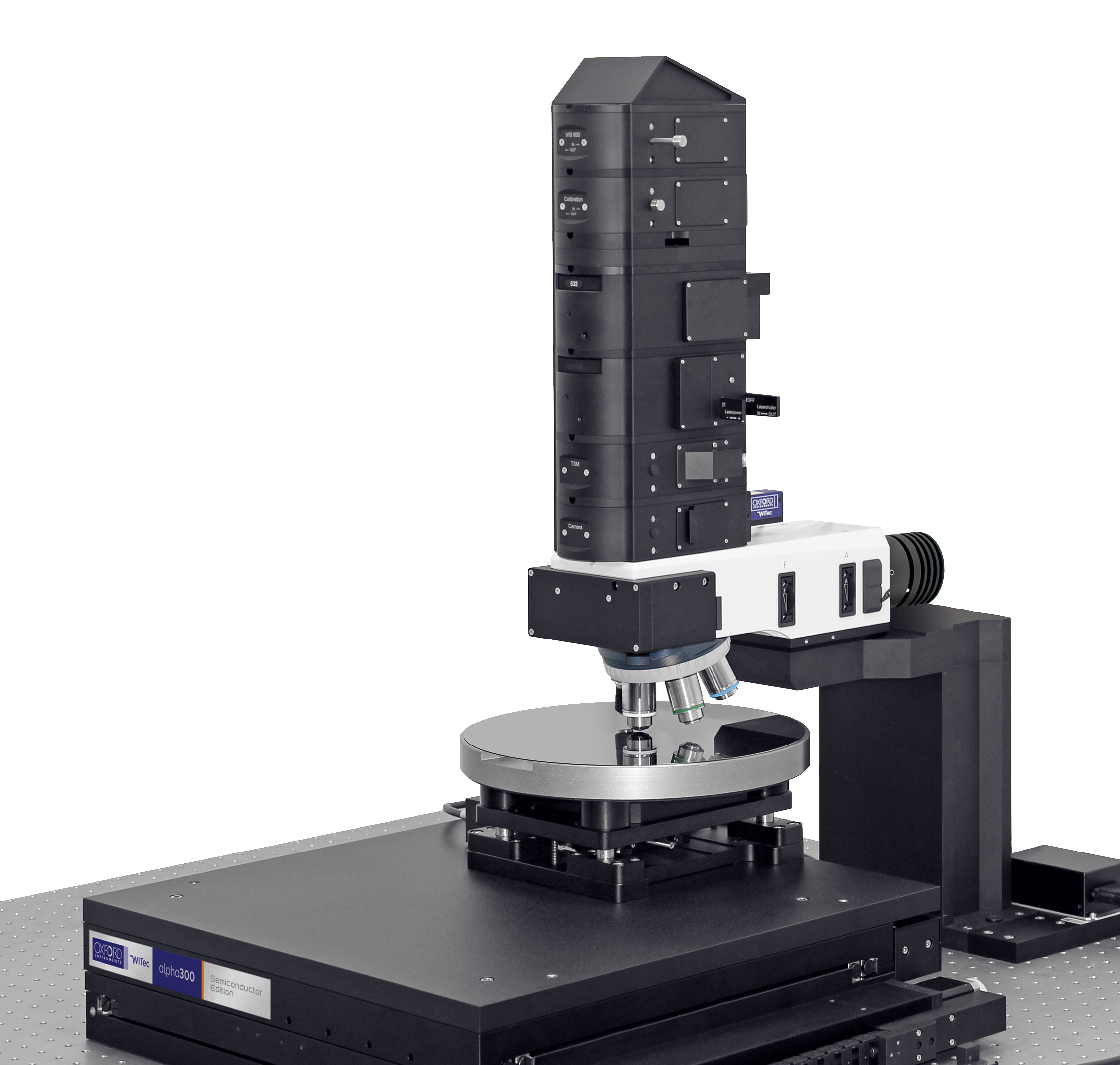
Figure 1: WITec alpha300 Semiconductor Edition Raman microscope
The WITec alpha300 Semiconductor Edition facilitates the assessment of entire wafers. It integrates our
industry-leading technology for Raman and PL measurements and is optimally equipped for large-area scans. An
extended-range scanning stage enables Raman imaging of wafers up to 300 mm (12 inch). The integrated
topography-compensating TrueSurface profilometry module stabilizes the imaging throughout measurements with long
acquisition times. TrueSurface additionally records the material‘s topography and warpage simultaneously with the
imaging.
| INFO BOX
|
|
What is photoluminescence?
In photoluminescence (PL), molecules absorb a photon of incoming light, which leads to the excitation of an electron to a higher energy level. In the excited state, internal relaxation processes can occur before the electron returns to its energetic ground state and a photon is emitted. The energy and wavelength of the emitted light corresponds with the difference of the excited and ground state energy levels in the molecule or crystal. The emission wavelength in PL is characteristic for the properties of a material. |
Why is PL useful for semiconductor analysis?
Semiconductors are a class of materials that are generally PL-active. Electrons in semiconductors can be excited for PL with light of a higher energy than the bandgap. This creates electron-hole pairs in the conduction and valence bands. The restoration process of the initial state causes the emission of a photon. Due to relaxation processes in the exited state, the energy of the radiated light lies in the range of the semiconductor‘s bandgap. Determining the wavelength of the semiconductor‘s PL-emitted light can thus serve as an indicator for its electronic features and allow conclusions on its bandgap. |
Correlative imaging of entire wafers
Thin, large diameter wafers form the basis for the fabrication of integrated circuits. The assessment of their
characteristics in the initial state and after different steps in the manufacturing process is essential, as their
electronic properties set the foundation for the functionality of the final product. In the following we present the
application of confocal Raman microscopy to analyze material characteristics including doping, stress fields,
crystallinity and warpage of a silicon carbide (SiC) wafer. To maintain this nanoscale-precision across the
macroscopically large x and y dimensions of an entire wafer, we used the WITec alpha300 Semiconductor Edition Raman
microscope (Fig. 1). This allowed us to perform a correlative imaging of the complete surface of a 150 mm (6 inch) SiC
wafer. The wafer area was Raman-imaged at a resolution of 1200 x 450 pixels using a 532 nm laser at 59.5 mW and a
20x/0.5 NA objective.
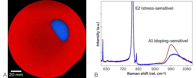
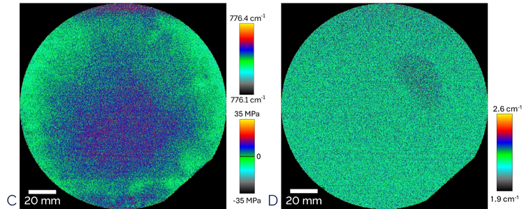
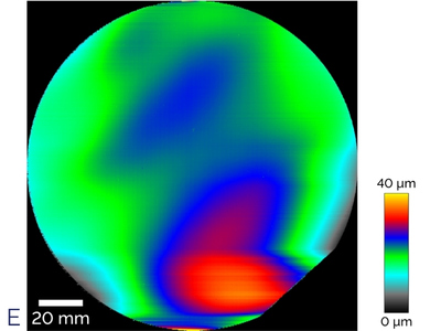
Figure 2: Raman imaging of a SiC wafer. (A) Confocal Raman imaging visualizes the
crystal facet region with a different doping concentration (blue) compared to the bulk area (red) in a 150 mm SiC
wafer. The coloration and identification are based on the analysis of the Raman spectra as given in (B).
(B) Raman spectra ofthe two identified components. They mainly differ in the
doping-sensitive A1(LO) mode (ca. 990 cm-1 relative
wavenumbers). (C) Color-codedposition of the stress-sensitive
E2(high) peak (776 cm-1) in the SiC wafer. The image
reveals compressive stress-induced peak shifts in the wafer’s center and tensile stress shifts toward its edge. A
second scale gives the calculated stress values in MPa. The zero stress value is defined by the average of the
stress distribution. (D) Crystallinity of SiC based on the FWHM of the
E2(high) peak. The wafer shows minor changes in its crystalline structure in the facet
region. (E) Warpage of the SiC wafer with height variations of up to 40 μm.
Doping
Raman imaging revealed differences in the semiconductor doping for a region close to the center of the wafer, which
represents the growth facet region (Fig. 2A, blue). Here, the spectral data (Fig. 2B) shows a peak shift and
broadening for the doping-sensitive A1(LO) mode at 960 cm-1 (relative wavenumbers). This is the
result of a higher doping concentration that increases the phonon-plasmon coupling and causes a shift to the LO
plasmon-coupled (LOPC) mode [1].
Stress and strain
The spectral data also resolved areas of compressive and tensile stress in the wafer. Due to the system‘s
sensitivity, we were able to determine the exact spectral position of the stress and strain- sensitive
E2(high) mode at 776 cm-1. In comparison to the overall wafer, more central regions were exposed
to compressive stress (Fig. 2C). This is indicated by a E2(high) peak shift towards higher wavenumbers [2].
In contrast, distal regions were subjected to relatively higher tensile stress. The stress can also be quantified and
calculated in absolute values in MPa with reference values for the material.
Crystallinity
Conclusions on the crystalline structure of the material can be drawn from the full width half maximum (FWHM) of the
E2(high) Raman band. Higher levels of crystallinity result in a thinner peak. This wafer showed an overall
homogeneous structure except for a slightly decreased crystallinity in the facet region (Fig. 2D).
Topography and warpage
The microscope‘s TrueSurface module compensated for height variations in the sample during the Raman imaging. The
recording of these z-position data allows for a correlative inspection of the sample‘s topography and warpage. The
analyzed wafer had a curved warpage with height variations up to 40 μm (Fig. 2E).
Beneath the surface: Raman depth-scans
The hexagonal polytype of silicon carbide (4H-SiC) is one of the most common semiconductor crystals used in wafers.
As it is transparent for light in the green spectral range, analyses of the material’s interior are possible with
optical techniques. Here, we used Raman imaging and a 532 nm laser to characterize the profile of a processed 4H-SiC
wafer. The examined wafer was processed by our Oxford Instruments colleagues from Plasma Technology with three
subsequent treatments: a mechanical polishing (MP), a plasma treatment (PPDE), and the growth of a crystalline SiC
layer on the top. For the profile analysis, we performed a Raman depth scan in a central region of the intact wafer.
Raman spectra were collected from 40 x 200 pixels of a 10 x 20 μm2 area using a 100x/0.9 NA objective.
A TrueComponent Analysis of the Raman data identified three layers (Fig. 3A). The bottom substrate layer (blue) and
top epitaxial layer (red) were separated by a thin buffer layer (green). The components differed in their Raman
spectra in the doping-sensitive A1(LO)/LOPC bands at 960 cm-1 and 990 cm-1 (relative
wavenumbers, see Fig. 3B). The substrate layer (blue spectrum) showed a decreased signal for the A1(LO)
mode and a shift towards the LOPC mode. This reveals the relatively higher doping concentration in the substrate
compared to the other layers [1]. The lowest doping concentration and purest A1(LO) spectrum was detected
in the epitaxial layer (red spectrum).
The results of the depth scan were used in a second step to determine the absolute thickness of the grown SiC
epitaxial layer. It was calculated from the measured width of the epilayer by including the refractive index of SiC
(n=2.635). The calculated thickness of the epitaxial layer was approximately 9 μm, combined with the buffer layer, it
spanned 10 μm.
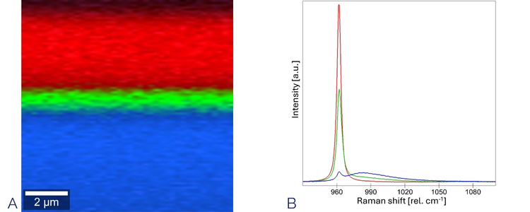
Figure 3: Depth scan of a SiC wafer. (A) Raman imaging and TrueComponent Analysis
identified a substrate layer (blue), buffer layer (green) and an epitaxial layer (red) of 4H-SiC.
(B) Respective Raman spectra of the identified components in the spectral range of
the doping-sensitive A1(LO)/LOPC Raman bands. Color-coding as in (A). The substrate
layer showed an assymmetrically widened, peak shifted to higher wavelengths.
Excursus: Novel 2D semiconductor materials
A new group of 2D materials that includes graphene, perovskite, molybdenum disulfide (MoS2), tungsten
diselenide (WSe2) and other transition metal dichalcogenides (TMDs) has recently been attracting attention
in the electronics industry. These few- to single-layered materials have novel properties which are exploited for
their structural, electronic and optical characteristics. Confocal Raman imaging is a preferred choice for the
non-destructive analysis of these 2D materials and the heterostructures formed by them. Our team analyzed
WSe2 crystals in a correlative approach with Raman, photoluminescence (PL) and second harmonic generation
(SHG) imaging. This revealed multilayering in the crystals and bandgap differences, and visualized grain boundaries.
Read more in our application note on correlative high-resolution imaging of TMDs
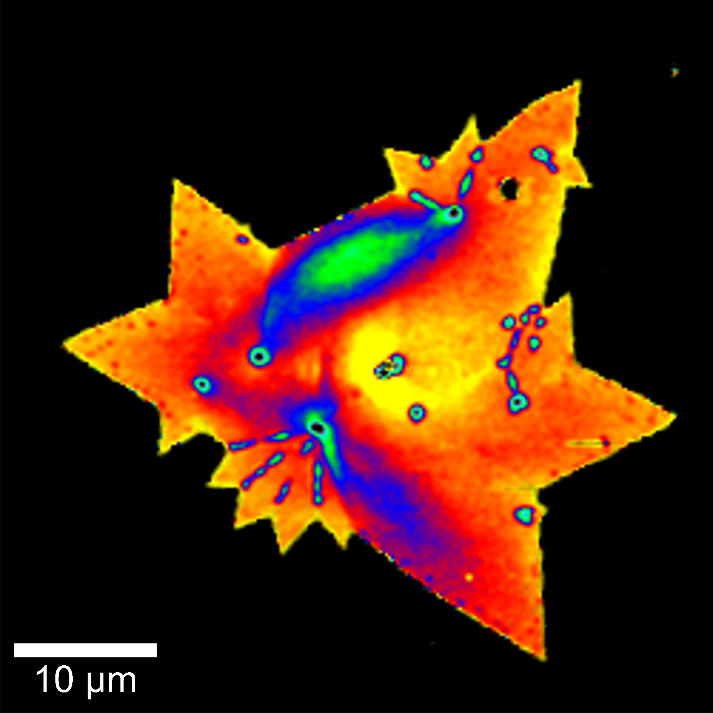
Figure 4: Raman image of MoS2
Raman and PL - Correlative analysis of wafer defects
The reliable detection and characterization of defects in wafers is a critical step in the early development of
electronic devices. Even the smallest alterations in the semiconductor crystal structure can drastically impact the
electronic properties and functionality of the final device. Here we used correlative Raman and photoluminescence (PL)
imaging to analyze alterations in a 4H-SiC wafer. The project was a cooperation with our colleagues from Oxford
Instruments Plasma Technology, who prepared the 150 mm wafer as described before.
Defect analysis with Raman
To quickly find the sites of material alterations and defects in the wafer, we performed a fast whole-wafer Raman
scan with the following settings: Laser excitation wavelength 532 nm, laser power 52 mW, 100x/0.9 NA objective, scan
area 155 x 147.5 mm2, resolution 1033 x 100 pixels.
As visible in Fig. 5A, some areas (cyan) were identified using TrueComponent Analysis as consisting of different
components than the overall material (red). The bright-field image of one of these areas visualized small triangular
structures on the surface of the wafer (Fig. 5B). With high-resolution Raman imaging (1000 x 750 μm², 200 x 150
pixels), these structures were easily detected and further analyzed (Fig. 5C). In contrast to the overall 4H-SiC
crystal, the visible structures had Raman spectral characteristics of the SiC polymorph 3C (Fig. 5D). The two forms
differed especially in their ratio of the Raman band intensities for the E2(high)-mode and
E1(TO)-mode. Due to the transparent properties of the material at the excitation wavelength of 532 nm, it
was possible to perform a 3D scan of the site with defects (Fig. 5E). This revealed that the origin for the surface
defects lies in the substrate layer (blue) of the wafer. Here, the defect was a thin, line- shaped area (carrot
defect). In the grown SiC epilayer, these defects propagated and developed further, forming triangle shapes as a
result of stacking faults.
Defect analysis with PL
The additional photoluminescence (PL) analysis revealed further imperfections in the wafer‘s surface along the
defects. The data acquisition was performed in the same area and at the identical resolution as the Raman imaging. PL
was excited using a 355 nm laser, which has a low penetration depth in SiC. This way, we were able to characterize the
surface effects without the influence of signals from lower material layers. To optimally detect the PL signals at
lower and higher wavelengths, two measurements from different ranges were combined (350 - 450 nm and 490 - 600 nm). As
a result, regions with different PL properties were revealed (Fig. 6A). In addition to the triangular areas in cyan,
which overlay with the structures visible in the bright-field image (see Fig. 5B), also other regions (yellow, blue,
green) had different bandgap properties than the overall 4H-SiC layer (red, Fig. 6B). The first three PL spectra are
specific for 4H-SiC with signs of stacking faults in the blue and green spectra [3]. Spectra obtained from the
triangular shaped defects (cyan and yellow) show typical PL of 3C-SiC [4].
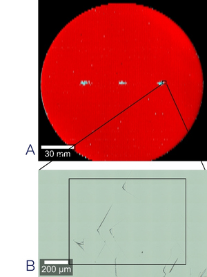
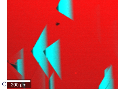
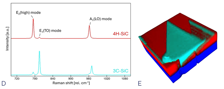
Figure 5: Raman-based detection of defects in a 4H-SiC wafer. (A) Raman scan image of
an entire 150 mm wafer. Small areas with structural differences (cyan) compared to the overall wafer (red) were
identified in the surface. (B) Bright-field image of the area indicated in (A)
visualizing triangular-shaped defects in the wafer‘s surface. (C) Highresolution
Raman image of the red-boxed area in (B). A different component (cyan) was identified in the triangular shapes of
the wafer surface. (D) Raman spectra of the found components; Color coding as in
(C). The spectra differ in their Raman peaks for the E2(high) and
E1(TO) modes and are characteristic for the 4H polymorph (red) and 3C polymorph (cyan)
of SiC. (E) 3D Raman representation of the defect (cyan) in the SiC crystal
layering. The alteration originates from a thin area in the substrate (blue) of the wafer and projects in the
epilayer (red). Dimensions: 240 x 240 x 12 μm3.
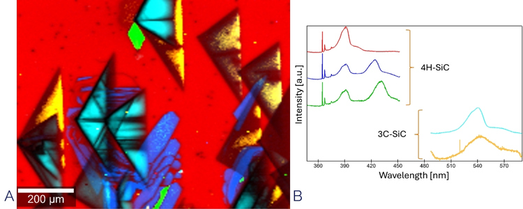
Figure 6: Photoluminescence-based detection of defects in a 4H-SiC wafer. (A) Combined
PL image of the defect site in the wafer (region as indicated in Fig. 5B). Areas with different PL signals can be
distinguished. (B) PL spectra of the identified areas. The red, blue and green
spectra show characteristics for 4H-SiC, spectra from the regions colored in yellow and cyan show signatures of
3C-SiC.
Detection of material stress in GaN with Raman
Material defects can severely affect the surrounding areas in the crystal lattice of semiconductors. In the presented
measurements, we used Raman imaging to investigate shear stresses in gallium nitride (GaN), which were induced by a
Frank-Read source (FR-source).
The brightfield image shows the characteristic dislocation loops of a FR-source in the material (Fig. 7A). The high
sensitivity of Raman imaging enabled the detection of changes in the position of the E2(high) peak of GaN
(Fig. 7D) and revealed areas of tensile and compressive stress (Fig. 7BC). The center of the FR-source showed the
highest tensile stress, but shear forces were also visible in surrounding areas.
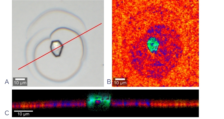
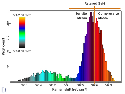
Figure 7: Frank-Read source in crystalline gallium nitride (GaN). (A) Brightfield image
of a Frank-Read (FR) source in gallium nitride (GaN). (B-C) Colored Raman images
of the E2(high) peak position in the xy plane (B) and along a line selection in the xz
direction (C). Color-coding as in (D). Due to the FR-source, areas of tensile and compressive stress are present in
GaN. (D) Histogram and color-coding of the E2(high)
peak position; Data of the sample region shown in (C). Wavenumbers below 567.6 cm-1
indicate tensile stress in GaN, while higher wavenumbers indicate compressive stress.
References
[1] Burton, J. C., et al., (1998). Spatial characterization of doped SiC wafers by Raman spectroscopy. Journal of
Applied Physics, 84(11), 6268-6273. DOI: 10.1063/1.368947
[2] Sugie, R., & Uchida, T. (2017). Determination of stress components in 4H-SiC power devices via Raman
spectroscopy. Journal of Applied Physics, 122(19). DOI: 10.1063/1.5003613
[3] Feng, G., et al. (2008). Characterization of stacking faults in 4H-SiC epilayers by room-temperature
microphotoluminescence mapping. Applied Physics Letters, 92(22). DOI: 10.1063/1.2937097
[4] Scuderi, V., et al. (2020). Characterization of 4H-and 6H-like stacking faults in cross section of 3C-SiC
epitaxial layer by room-temperature μ-photoluminescence and μ-raman analysis. Materials, 13(8), 1837. DOI:
10.3390/ma13081837

