Raman, SHG and PL imaging of an MoS2 flake
Two-dimensional (2D) materials such as transition metal dichalcogenides (TMDs) are receiving increasing attention due to their unique optical and electronic properties. Their possible applications include the production of transistors, photo detectors, light emitting diodes (LEDs) and photovoltaic cells. In order to produce high-quality devices, synthesis processes must be evaluated efficiently. Thus, non-destructive imaging techniques are required for monitoring crystal properties and features such as grain boundaries, layer number, defect density, doping and strain fields.
The following measurement of CVD-grown mono-layer molybdenum disulfide (MoS2) illustrates the advantages of correlative Raman, second harmonic generation (SHG) and photoluminescence (PL) microscopy for investigating TMDs. All measurements were performed at the same area of interest using a WITec alpha300 microscope equipped with a 532 nm laser for Raman and PL imaging and a picosecond-pulsed 1064 nm laser for SHG excitation.
In the white-light image (A), the contour of an MoS2 flake is visible, but no further features can be discerned other than a few bright spots caused by local bulk material. In contrast, Raman, SHG and PL imaging can reveal details about the material's structure and quality.
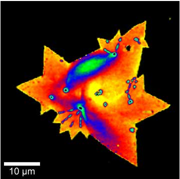
Fig. A — White-light image of the MoS2 flake showing the overall contour and a few bright spots of local bulk material.
Second Harmonic Generation (SHG) Imaging
Second harmonic generation (SHG) microscopy is a cutting-edge imaging technique for the investigation of TMDs. SHG is a nonlinear optical process that radiates a photon with twice the frequency of the excitation photon and is sensitive to changes in crystal orientation and symmetry [1, 2]. The high-resolution SHG intensity image (B) clearly visualizes the grain boundaries in the MoS2 flake (low SHG signal), as well as areas with increased signal. In order to evaluate the optical resolution of the measurement, a Lorentzian function was fitted to the intensity profile along the cross-section over one grain boundary. The obtained full width at half maximum of about 630 nm is close to the diffraction limited resolution of about 590 nm that can be achieved with 1064 nm excitation and a 0.9 NA objective.
In addition, polarization-dependent SHG measurements can identify the crystal orientation and reveal strain fields [1, 3]. To this end, the excitation polarization is rotated while recording the intensity of the SHG signal component that has the same polarization as the incident light. Due to the fully automated polarizer and analyzer operation of the microscope used, polarization-dependent measurements can be performed automatically within seconds. Polarization series were recorded at three positions of the MoS2 flake (B) and represented in polar plots that depict the recorded SHG signal as a function of the excitation polarization angle (C). A particularly symmetric pattern is observed for the position marked in red, indicating little strain in the crystal [3]. In contrast, the other two positions show distinct asymmetric patterns representing different strain levels.
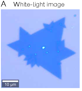
Fig. B–C — (B) SHG intensity image of the MoS2 flake with three marked measurement positions. (C) Polar plots of the SHG signal as a function of excitation polarization angle at the three indicated positions.
Raman Imaging
Raman imaging can reveal strain fields in crystals and quantify the number of layers in few-layer TMDs [4]. A typical Raman spectrum of MoS2 shows two prominent bands, the E2g band originating from an in-plane vibration and the A1g band originating from an out-of-plane vibration (D). Their exact positions were quantified for every image pixel by fitting a Lorentzian function and their respective frequencies were color-coded in Raman images (E, F). Grain boundaries are not visible in the Raman images, but some areas that showed increased SHG intensity also show a pronounced shift of the A1g and E2g bands. In the Raman image of the A1g frequency, rim effects are visible at the borders of the MoS2 flake, where the A1g band is the most strongly red-shifted (F). The frequency of the E2g band is particularly sensitive for strain in the crystal [4, 5]. The corresponding Raman image revealed two areas of strong tensile strain, indicated by a pronounced red-shift of the E2g band (E).
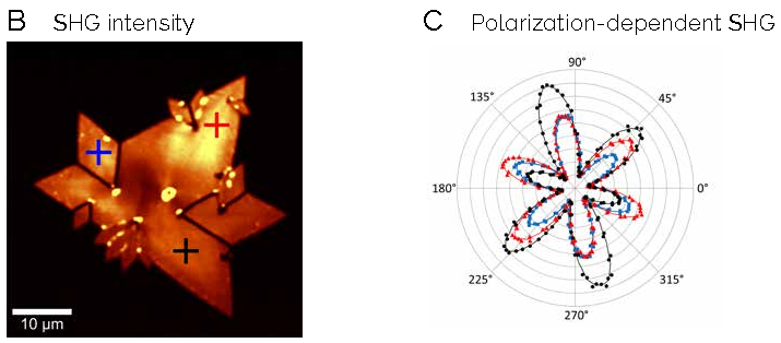
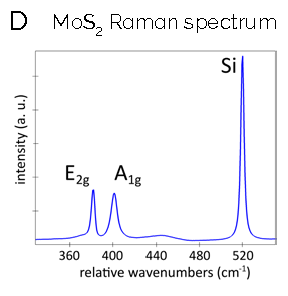
Fig. D — Raman spectrum of MoS2 on a silicon substrate, showing the E2g and A1g bands.
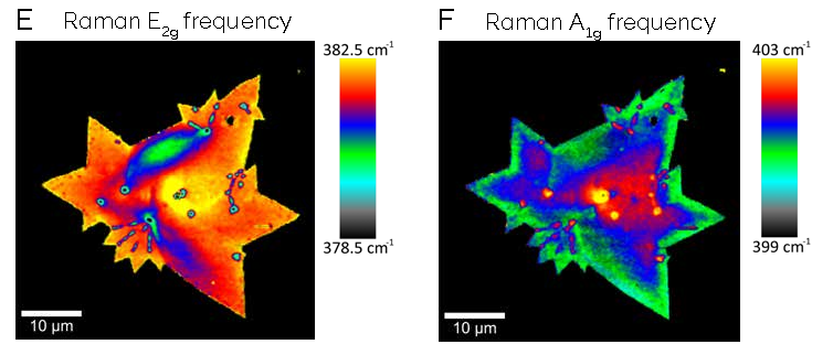
Fig. G–H — Photoluminescence images of the MoS2 flake representing signal intensity (G) and wavelength (H).
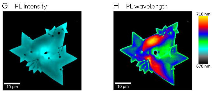
Fig. E–F — Raman images displaying the frequency of the E2g mode (E) and the A1g mode (F), color-coded per pixel across the MoS2 flake.
Photoluminescence (PL) Imaging
Photoluminescence imaging can be used for investigating strain, doping, defects and layer number in TMD crystals [6, 7]. Intensity, wavelength and width of the MoS2 flake's PL signal were fitted by a Lorentzian function and color-coded in the PL images (G, H, I). The PL intensity is increased at the rim of the flake and close to its center, while the spots that showed increased SHG signal correlate with low PL intensity (G). The rim effects are even more clearly visible from the pronounced blue-shift of the PL wavelength around the border of the MoS2 flake (H). The PL signal is also sensitive to strain [6, 7] and the PL wavelength shows a pronounced red-shift in the same areas as the Raman E2g frequency (E, H). This is also correlated with increased width of the PL signal (I).
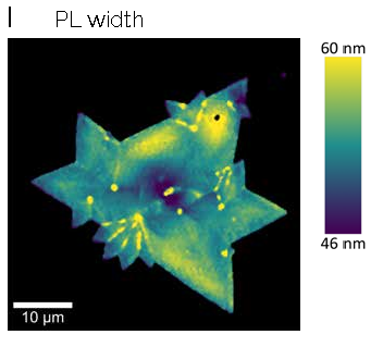
Fig. I — Photoluminescence image representing the signal width (I) across the MoS2 flake.Image size: 50 µm x 50 µm with 200 nm per pixel for all SHG, Raman and PL images. (A) White-light image. (B) SHG intensity image. Polarization series (C) were recorded at the three indicated positions. (C) Polar plots of the SHG signal as a function of the excitation polarization angle at the three positions indicated in (B). The intensity refers to the SHG component that has the same polarization as the incident light. (D) Raman spectrum of MoS2 on a silicon substrate. (E–F) Raman images displaying the frequency of the E2g mode (E) and the A1g mode (F). (G–I) Photoluminescence images representing the signal intensity (G), wavelength (H) and width (I).
Correlative Raman, PL and SHG imaging yields complementary and consistent information for characterizing single-layer TMD crystals by visualizing features of the crystal structure, such as grain boundaries or strain fields, without damaging the sample.
References
- Y. Wang et al. (2019). Second harmonic generation spectroscopy on two-dimensional materials. Opt Mater. Express, 9: 1136–1149.
- L. Karvonen et al. (2017). Rapid visualization of grain boundaries in monolayer MoS2 by multi-photon microscopy. Nat. Commun., 8: 15714.
- L. Mennel et al. (2018). Optical imaging of strain in two-dimensional crystals. Nat. Commun., 9: 516.
- H. Hu et al. Low frequency Raman scattering of two-dimensional materials beyond graphene. In Confocal Raman Microscopy, J. Toporski, T. Dieing, O. Hollricher (eds.). Springer Series in Surface Sciences 66, Springer International Publishing AG, 2nd ed., 2018, pp. 195–206.
- Y. Wang et al. (2013). Raman spectroscopy study of lattice vibration and crystallographic orientation of monolayer MoS2 under uniaxial strain. Small, 9: 2857–2861.
- S. Luo et al. (2020). Investigation of growth-induced strain in monolayer MoS2 grown by chemical vapor deposition. Appl. Surf. Sci., 508: 145126.
- Z. Liu et al. (2014). Strain and structure heterogeneity in MoS2 atomic layers grown by chemical vapour deposition. Nat. Commun., 5: 5246.

