One of the most common questions I receive as TEM product manager is, “What’s the difference between TEM EDS and SEM EDS?”. This is an extremely valid question, especially as in both scenarios we are using the same mechanism to produce the same X-rays for detection using the same detector* (from a technology point of view). To answer this, it is best to break down our response into 3 key areas: the sample, the hardware and the software.
The Sample
A common mistake when comparing scanning electron microscopy (SEM) to transmission electron microscopy (TEM) is the assumption that you are looking at the “same” sample in SEM as you are in TEM. Yes, from a technical point of view you are looking at the same material, however, as TEM requires electron transparent samples, with thicknesses typically <100 nm. So, the resulting sample is significantly changed from the bulk material it once was.
This is a key differentiator that is often overlooked. SEM analysis is predominantly a bulk
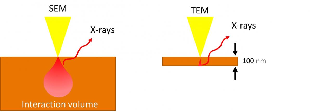
characterisation technique in which high accelerating voltages generate large X-ray interaction volumes to probe the microscale composition of a material, as shown below in Figure 1. This is why techniques like EDS and WDS are so widely used to calculate the composition of a material, as they provide a big picture response to what elements are present.
A real-world example of this is cake. When we eat cake, we taste cake, you get hints of flavour, be that lemon, fruit, jam, carrot, but the overall taste is the cake, and this is the same for bulk SEM EDS.
TEM is only a bulk characterisation technique when the material is naturally electron transparent and typically <100 nm in size, i.e. nanoparticles. For most samples, TEM provides a site specific/targeted characterisation to identify the local nanoscale composition. It allows you to analyse the building blocks of a material and how those trace components are interacting to form your bulk structure. Sticking with our cake analogy, we’ve taken a fork full of cake and smeared it out on the plate. Wow! we can actually see the individual pieces of lemon, fruit, jam and carrot, and taste them individually to be certain of those ingredients.

Figure 1. Visualisation of the interaction volumes being probed using SEM and TEM. The interaction volume is the source of our EDS X-rays.
The Hardware
SDD-based EDS detector hardware is the same in both SEM and TEM. However, there are some subtle nuances that greatly influence the number of X-rays a detector acquires and the resulting spectrum when comparing SEM to TEM.
Standard SEM detectors are positioned in a safe position above the SEM polepiece where they cannot be damaged by SEM stage collisions and have a clear line of site between the sample and the EDS detector. This is why, typically, SEM EDS configurations require the SEM to be operated at a large working distance. The detectors are built with a window in front of the SDD, protecting the SDD when the microscope is vente and this is required as SDD detectors operate at negative temperatures. If the SDD was exposed to air when cold, it could result in SDD damage. The exception to this is the Oxford Instruments Extreme which has been optimised to perform at low working distances and is windowless, much like a TEM detector.
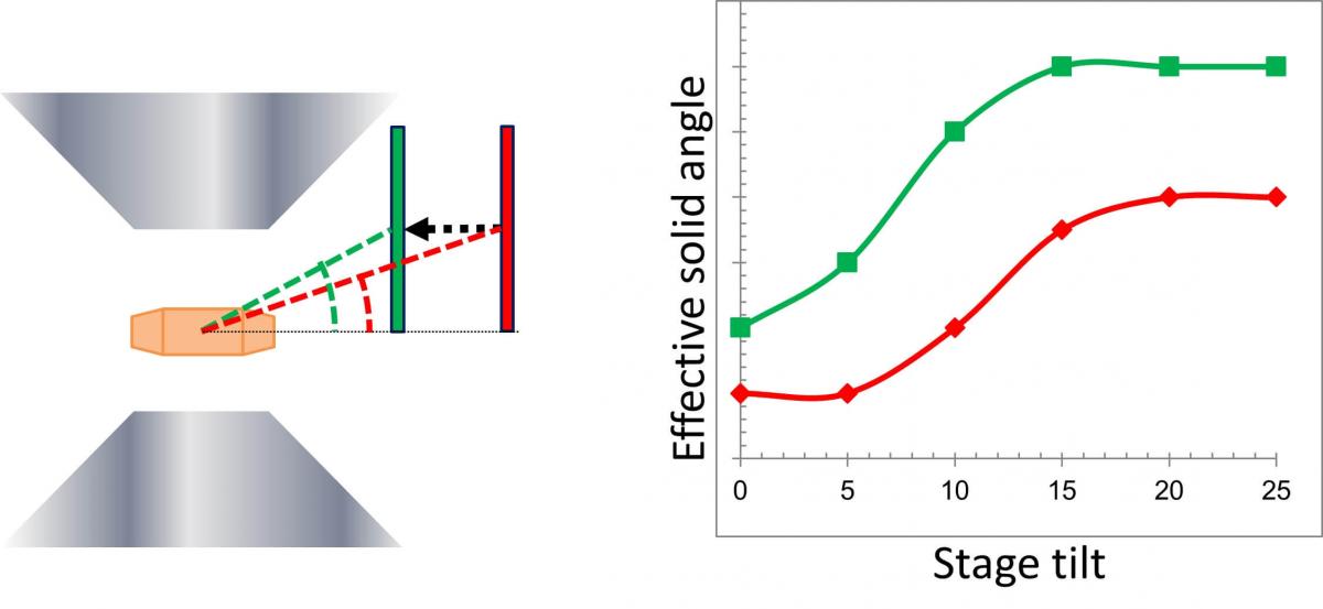
TEM detector positioning requires much greater levels of precision; the aim being to bring the EDS detector as close to the sample as possible. As TEM samples are inserted between the upper and lower polepieces, detectors are positioned above the plane of the sample holder, minimising detector shadowing to optimise the solid angle, even at 0° tilt, as shown below in Figure 2. Additionally, we more frequently use windowless detectors in TEM, as the column is rarely vented to air. This means we have lower SDD damage risk. This improves solid angle and results in greater sensitivity to low energy X-rays.
Figure 2. Effective solid angle as a function of TEM EDS detector positioning.
The Software
Finally, we can look at software. You may think that the only difference between SEM-EDS and TEM-EDS in AZtec is which button you click on in the selection box. This is an easy assumption to make, as you will have the same options in both modes, point & id, linescan, mapping. The big change that is applied is to the quantification routines that are being applied to the EDS data. I won’t go into the nitty gritty detail on these quantification routines here, but if interested, you should have a look at Simon’s blog comparing bulk SEM quant to STEM-SEM TEM quantification available here.
Fundamentally, we apply a bulk standardless quantification to SEM data whilst TEM applies a Cliff-Lorimer k factor quantification.
I hope you found this blog insightful and that it has challenged what you may have seen as a rather obvious question. I will be focussing on the TEM differences in my upcoming tutorial “An introduction to TEM EDS” and would welcome anyone to attend or watch on demand.