My previous blogs have introduced the WITec demo lab here in High Wycombe and looked at how Raman spectroscopy can be used alongside our NanoAnalysis products for material analysis. I want to take this time now to go through some of the history and fundamentals of Raman spectroscopy and confocal Raman imaging. Now, all those NanoAnalysis users out there, please bear with me as we swap our electron microscope for an optical one.
First up – A very brief history lesson
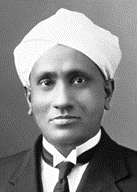
The story starts with Sir Chandrasekhara Venkata Raman, an Indian physicist who observed that light changes frequency when passing through transparent material, and it was for this discovery that he was awarded the Nobel Prize in Physics in 19301. Measuring these changes in frequency is the basis of Raman spectroscopy. The advent of modern laser and spectrometer systems has transformed the technique and it is now widely applied in the world of material characterisation.

Figure 1: C.V. Raman
Raman Scattering – Basic Principles
Don’t worry, this explanation won’t dive too deeply into the physics of the interaction, and there won’t be any form of test at the end! For some, this might be a refresher but, I also appreciate that this might be somewhat new to some readers out there.
First up, we need to hit our molecule with a photon of light existing as a packet of energy.
Three processes occur when this happens:
- The photon might simply pass straight through the molecule causing no change whatsoever.
- The molecule might absorb this little packet of energy which changes the energy of the molecule.
- The photon might be scattered.
And it is this scattering process that we are interested in. Most of the time, this photon is scattered without any energy change, and we call that Rayleigh Scatter – this is the reason why the sky is blue!
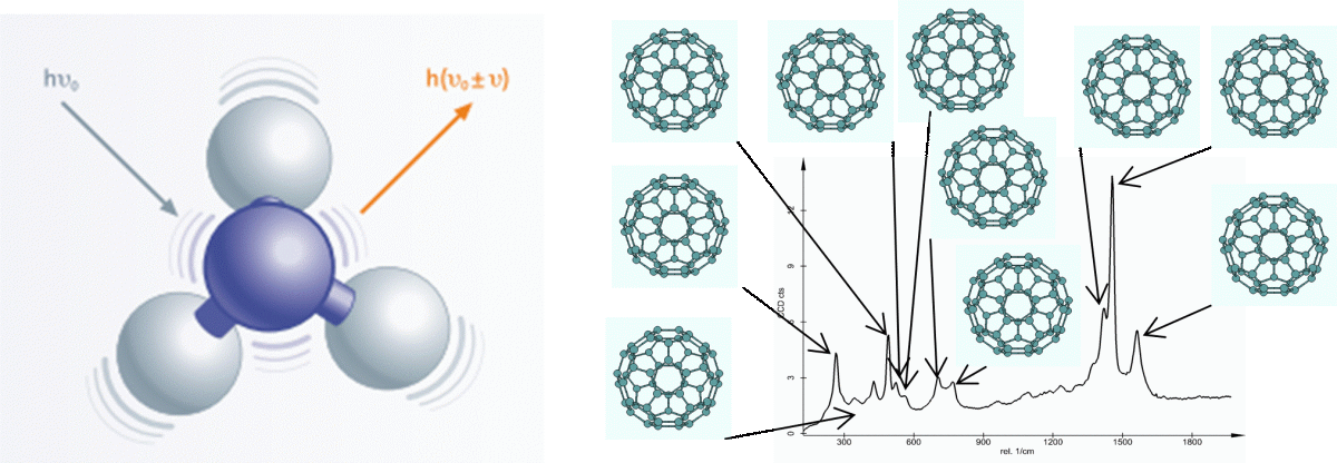
In very rare cases, this photon might excite the molecule just slightly, causing the molecule to vibrate and changing the energy of the photon. This is our Raman scatter.

Figure 2 a: A representation of what happens during and Raman Scattering event and b: The vibrational modes of Buckminster Fullerene, C60 and where they are found on the Raman spectrum
Molecular vibrations can get quite complex, but if we imagine 2 atoms bound together as 2 balls connected by a spring. That bond in the middle can move in a variety of ways including stretching and bending. It is these movements that occur when a molecule vibrates, and the energy change or shift of the photon reflects both the type of vibration and the particular atoms involved. Our Raman spectrum is made up of every single one of these Raman-active vibrations that occur within our molecule.
How do we get Raman Scatter?
To generate our Raman scatter, we must bombard our molecule with enough light, so this incredibly rare event occurs often enough to capture it. This is where lasers are incredibly useful, as they emit light of a single wavelength at a consistent energy, meaning we can identify the photons that have shifted in energy. Our WITec systems use confocal optical microscopes to focus this laser light into a highly spatially resolved spot on our material. This means we only excite that particular area and capture the Raman scatter from that point. By analysing multiple points in a field of view we can map our surfaces and distinguish the different chemical components within the material. We can also obtain 3-dimensional information so long as the laser can penetrate the material.
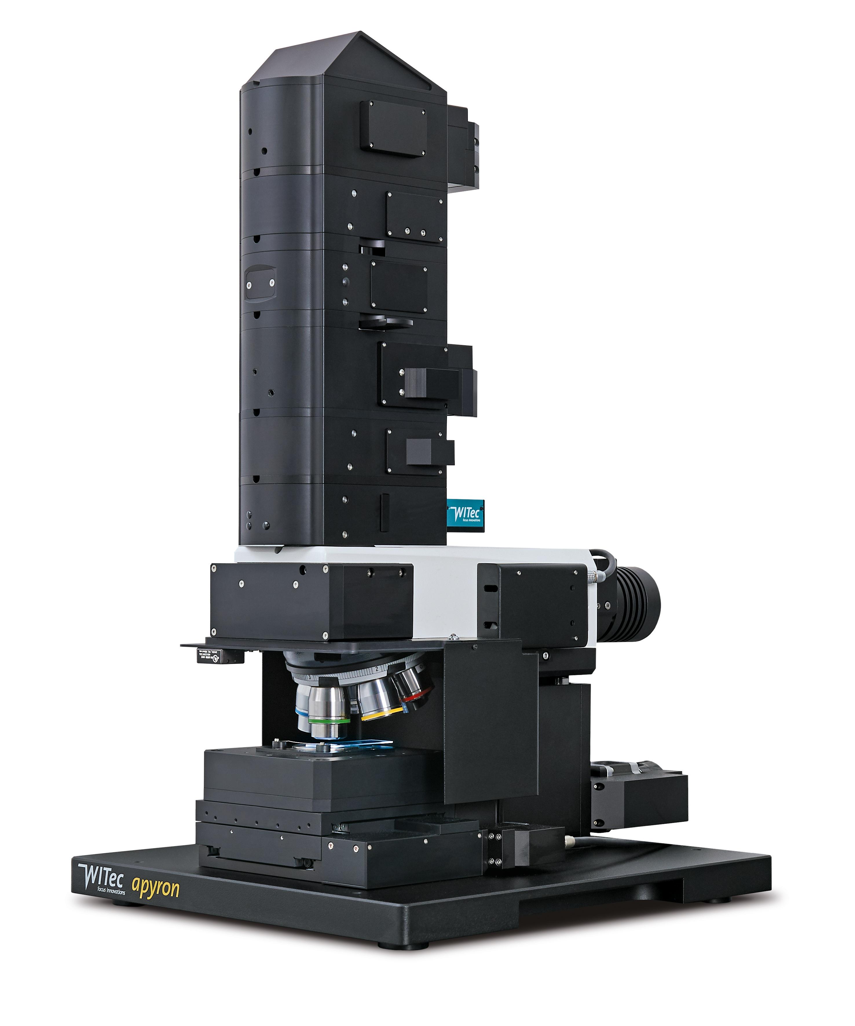
Figure 3: The Oxford Instruments Apyron Raman Microscope
What does Raman give us?
I mentioned before that a Raman spectrum is comprised of all the Raman active vibrations that occur within our molecule – we refer to this as our Raman fingerprint. Now as the name suggests, we can use this fingerprint to identify components of a mixture by their spectrum. But that isn’t all we can see, as our spectrum can also provide other insights into our material. For instance, peak intensity provides us with information on the quantity of a component, while any shifts in the vibration can indicate stress and strain states. We can also deduce the crystalline properties of the material from peak width and orientation from the polarisation state.
What can we analyse with Raman Spectroscopy?
Essentially, if a sample scatters light, then we can analyse it, meaning we can apply Raman spectroscopy to a wide range of samples with little to no preparation. An additional and significant benefit of this is that Raman is a non-destructive technique. Because of this, Raman spectroscopy has been used to analyse a wide range of materials from meteorites to Renaissance art. It can identify the components of living cells and showed us the self-healing properties of Roman concrete.
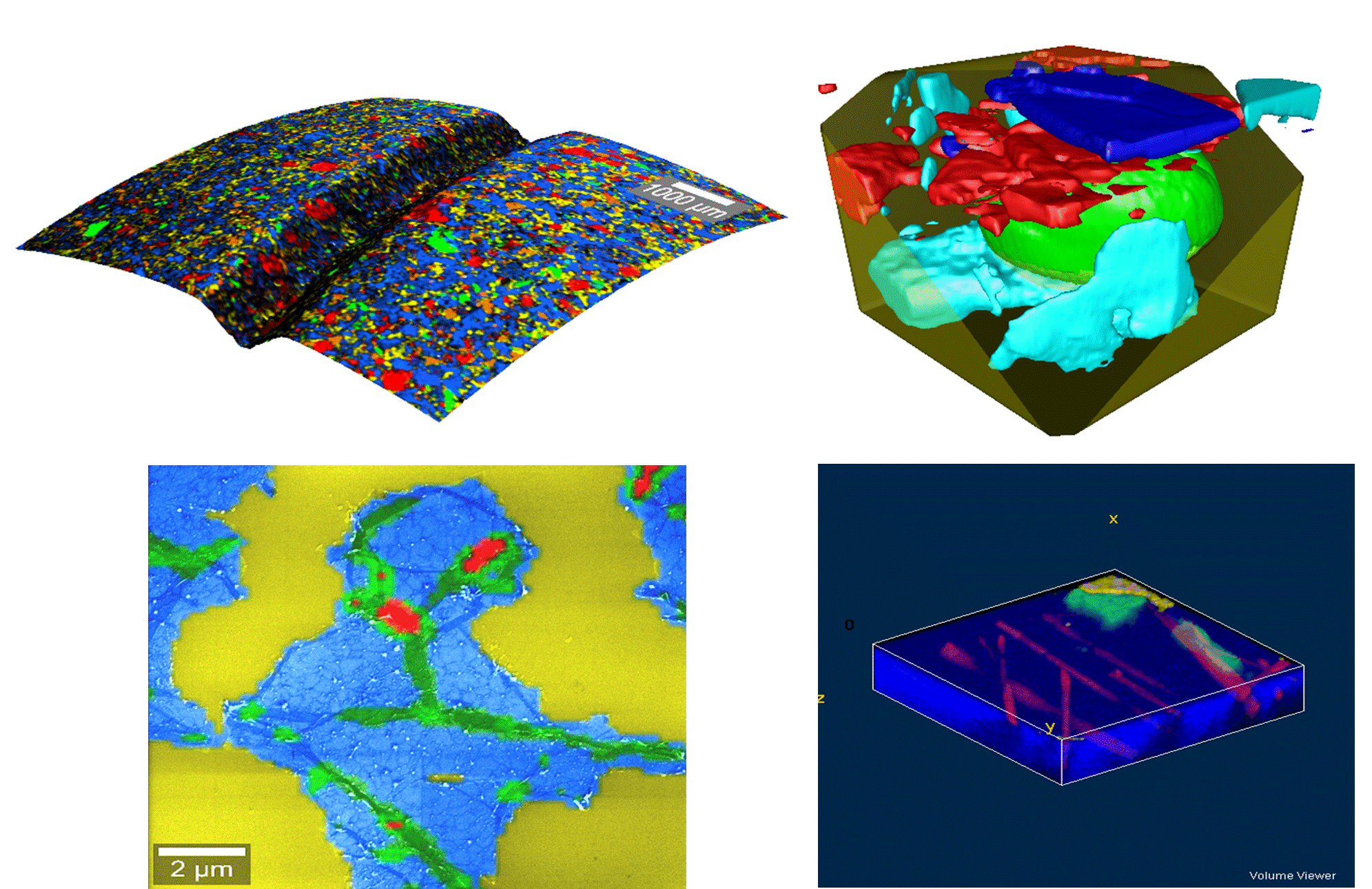
Figure 4: clockwise starting top left a. Large area topographical map of a tablet. b. A 3D scan of a pollen grain suspended in crystalline honey – the red, blue and cyan colours represent different crystalline honey phases. c. An animation of 3D scan showing asbestos inclusions in a mineral matrix 2 d. Raman map of graphene showing the different layers and wrinkles.
How does Raman compare to and complement EDS?
Those of you who are reading this are perhaps very aware of the information that EDS can deliver, but I will provide a brief description for the purposes of demonstrating how Raman imaging is similar in some regards and different in others. However, the most important thing to remember is that the techniques are complementary, which really works in our favour.
EDS is reliant on the interaction of an electron beam with our sample which in turn produces characteristic X-rays showing us elemental distribution with quantitative information. We then take this data at precise points or pixels and process it into a nice false-colour map that shows us which elements are found in which pixel.
In a similar fashion, Raman uses an irradiation source (our laser) that interacts with our sample causing our scatter. This scatter is characteristic of the vibrational modes within our molecule, giving us our spectrum. We take a Raman spectrum at each pixel and process the data to show which molecule or component appears in each specific pixel. We can then generate a nice false-colour image where instead of elemental information, we get molecular information.
Now when I say that we get complementary data, what we mean is Raman is able to offer an additional perspective to our materials analysis. An example in which this is most apparent is the analysis of polymers. The information we get from EDS means we can identify where a polymer exists in a matrix but identifying the polymer structure is not possible. With Raman, we get the molecular information, giving us a more complete picture.
So, there you have it. A whistlestop tour of Raman spectroscopy that has taken you through the history and principles of this fascinating form of analysis. I have described how we obtain a Raman spectrum with a brief look into the science of it all. I also demonstrated what we can analyse and hopefully now you also see how useful it can be when aligned with our EDS analysis.
Thank you for reading!
More information can be found here: https://raman.oxinst.com/learning/view/article/raman-knowledge-base
References
- C. V. Raman and K. S. Krishnan, Nature, 1928, 122, 12–13.
- 2. G. Wille, D. Lahondere, U. Schmidt, J. Duron and X. Bourrat, Journal of Hazardous Materials, 2019, 374, 447–458.