17 Jul
Introducing the ALD plasma processing system for 2D materials
Oxford Instruments’ ALD and 2D technical specialists have teamed with the Eindhoven University of Technology research teams to realise atomic layer deposition (ALD) of 2D transition metal dichalcogenides for nanodevice applications.
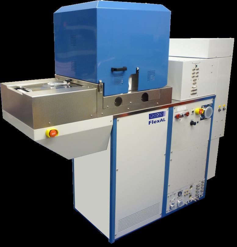
To this end a specific Oxford Instruments FlexAL ALD system configuration has been put together aimed at the growth of these 2D materials. The FlexAL-2D ALD system offers a number of benefits for growth of 2D materials:
- H2S plasma and H2S gas dosing
- Load-lock and turbo-pump for clean growth and working conditions
- Growth on 200 mm wafers
- Growth of ALD dielectrics and other ALD layers on 2D materials in same tool
- High temperature table (RT-600 °C)
- Plasma cleaning and conditioning of chamber
- RF substrate biasing option for further process flexibility
- In situ process monitoring option using spectroscopic ellipsometry and mass spectrometry
Atomic Layer Deposition (ALD) is a true nanotechnology, allowing ultra-thin films of a few nanometres to be deposited in a precisely controlled way. There are two defining characteristics of Atomic Layer Deposition, self-limiting atomic layer-by-layer growth and highly conformal coating. These characteristics have offered many benefits in semiconductor engineering, MEMS and other nanotechnology applications.
The expectation is that the wide parameter space offered by the FlexAL-2D ALD system should allow growth of 2D transition metal dichalcogenides already at lower temperatures than employed in CVD furnaces. The ability to do both H2S plasma and pure H2S gas should also provide direct sulfurzation pathways besides using it in ALD processing. First results on the growth of 2D MoS2 material by ALD at 450°C and lower temperatures was presented on July 16th 2017 by Eindhoven researchers at the ALD conference in Denver.
Chris Hodson, ALD Product Manager at Oxford Instruments Plasma Technology is delighted with this research, “Dr. Bol and the Plasma & Materials Processing (PMP) group at TU/e are pushing the boundaries of ALD research into new application areas. 2D materials are a hot topic and utilising ALD to allow growth at lower temperatures and combine 2D materials with ALD deposition and other processing methods at 200 mm provide a new capability with many possibilities.
Dr. Ageeth Bol comment, “We are excited about the results from the new ALD FlexAL configuration from Oxford Instruments, which has been configured to meet our needs.” Bol explains. The researchers are particularly interested in relatively low temperatures. “For CVD processes, typically temperatures of over a 1000 degrees Celsius are needed. That is often fatal for applications in semiconductors because the high temperature increases the diffusion of the atoms, which makes it harder to place them at the right spot. We want to have a process that yields materials of high quality at lower temperatures. This is especially important for the two-dimensional heterogeneous layers I am working on, since at lower temperatures less diffusion of atoms between the layers will occur.”