

14 Jun
New Application Note Details CharacterizingEmerging Photovoltaic Materials with Atomic Force Microscopy
Encouraging more widespread adoption of solar cells as a renewable and sustainable energy resource hinges upon reducing costs and increasing conversion efficiency. To achieve these goals, photovoltaic (PV) materials such as hybrid organic-inorganic perovskites and organic semiconductors hold promise for next-generation devices. Understanding the nanoscale properties of these emerging materials is critical in optimizing their performance. The atomic force microscope (AFM) is superbly suited for this purpose, measuring nanoscale structure and electrical behavior to gain deeper insight into relations between structure, properties, processing, and performance. The new application note “AFM Characterization of Emerging Photovoltaics” from Oxford Instruments Asylum Research discusses how AFMs are being used to image nanoscale electrical and functional response and map morphology in perovskites and organic materials. It also highlights the exclusive features, benefits, and operating modes of Asylum Research AFMs that enable successful materials characterization. The application note can be downloaded here.
“This application note is a must-read if you’re a scientist using AFM for photovoltaic applications or if you plan to integrate AFM into your research,” said Jason Li, Applications Manager, Asylum Research. “Exciting new results examples are presented from the world’s leading researchers who are at the forefront of developing next-generation solar-cell materials and devices with Asylum Research AFMs.”
Asylum Research Cypher and MFP-3D AFMs offer high resolution, easy operation, and a wide variety of functional imaging modes. Specifically designed or this application, the Photovoltaics Option for the MFP-3D Infinity AFM offers a flexible, turnkey platform featuring a customizable, bottom-side sample illumination. Asylum AFMs are easily configured for use in a glovebox and have a wide variety of accessories for remarkable environmental control for oxygen-and water-sensitive PV materials.
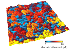
Figure caption: Nanoscale photoresponse image showing short-circuit current ISC overlaid on topography for a methylammonium lead triiodide (CH3NH3PbI3 or MAPbI3) film under ~0.07 W/cm2 illumination. Adapted from Y. Kutes, Y. Zhou, J. L. Bosse, J. Steffes, N. P. Padture, and B. D. Huey, Nano Lett. 16, 3434 (2016).