Introduction
Oxford Instruments Plasma Technology has developed an innovative set of plasma process solutions designed to enable maximum Silicon Carbide (SiC) device performance. SiC has a uniquely desirable set of properties for power device manufacture and is being progressively applied to achieve the breakthrough performance required to enable new and exciting technologies. A wide band gap semiconductor, SiC offers a high breakdown field and high thermal conductivity. These inherent advantages enable the production of power devices that answer closely to pressing industrial requirements for smaller, lighter, more efficient technology with the ability to operate at high temperatures. SiC power devices already have established benefit, and a considerable market, in power supply/power factor correction and photovoltaic applications. On the near horizon are electric and hybrid vehicles (EV and HV) and the associated infrastructure. Long term, the scope for substantial efficiency savings is considerable and extends well beyond these key applications.
In this white paper we consider the role of plasma processing and its importance in defining device performance and optimal strategies for the application. We also examine the structure of primary SiC devices such as Schottky barrier diodes (SBDs) and Metal Oxide Semiconductor Field Effect Transistors (MOSFETs).
The Impact of Switching to SiC
In electronic power circuits, power semiconductor devices perform the function of switches, rectifiers or amplifiers. Devices routinely used include SBDs, MOSFETs, bipolar junction transistors (BJTs), junction FETs (JFETs) and insulated gate bipolar transistors (IGBTs). A shared characteristic of many of these devices is that when 'off' they must resist the reverse flow of current ie. have a high reverse breakdown voltage. Conversely, 'on' resistance is preferentially very low, to minimise heat/power loss.
| Parameter |
Si |
SiC |
| Bandgap energy (eV) |
1.12 |
3.26 |
| Thermal Conductivity (W/cm-K) |
1.5 |
3.5 – 4.9* |
| Breakdown field (MV/cm) |
0.3 |
3 |
Table 1: Comparing certain characteristics of SiC with those of Si shows how it is able to deliver breakthrough power device performance.
A comparison of certain properties of SiC and Si (see table 1) within this context highlights its potential for far superior performance. The most notable difference between SiC and Si is the ten-fold higher breakdown field which makes it far more effective at blocking voltage. This means that the drift layer within a power device, which is specified on the basis of the requirement to block voltage, can be much thinner. Alternatively, or in addition, doping levels can be higher. Doping of the drift layer reduces on resistance but at the same time compromises breakdown voltage. The higher breakdown field of SiC means that there is far more scope to balance these effects to achieve desirable device characteristics.
Other performance-defining properties of SiC include its bandgap energy and thermal conductivity. The bandgap energy of SiC is approximately three times that of Si making it more suitable for high temperature applications for which Si is limited by the potential for thermal ionization. On the other hand, high thermal conductivity, around three times that of Si depending on which crystal plane measurements are made in, means that heat generated during device operation can be dissipated efficiently. In practical terms this eases thermal management within the device, minimising any loss in performance as a result of temperature rise. These are particularly advantageous characteristics for high power applications.
In combination these properties enable the configuration and manufacture of compact, highly efficient power devices, especially for high voltage, high power and high frequency applications.
SiC Power Devices
The most widely commercialised SiC devices are Schottky diodes and MOSFETs but other devices such as JFETs and BJTs are also available. Reviewing the structures of these devices helps to elucidate the processing steps required for their manufacture.
Schottky Barrier Diode
The basic structure of a SBD has a simple metal-semiconductor junction (the Schottky barrier) as shown in figure 1. When a sufficiently high forward bias is applied electrons from the n- drift layer flow through the diode. Application of a reverse voltage stops current flow, though there is a level of reverse leakage. The degree of reverse leakage, the reverse voltage that can be resisted before the device allows current flow, switching speed (between passing current and blocking it), and the resistance of the device when current is flowing, are all defining features in terms of performance.
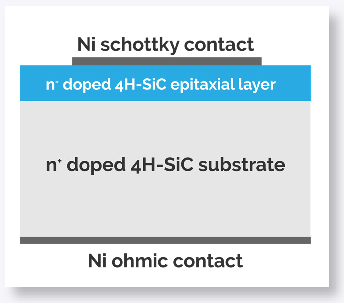 Fig. 1 — A basic SBD structure has the limitation that in reverse bias the peak electric field is coincidental with the metal-semiconductor interface, arguably the weakest point of the device.
An important disadvantage of this simple structure is that under reverse bias peak electrical field strength is coincidental with the metal-semiconductor interface. This is undesirable because it means that any structural defects at the interface, arising from, for example, imperfections in the epitaxial layer will have a significant impact on device performance. The introduction of submerged p+ wells eliminates this issue by moving the peak electric field to the base of the p+ wells (see figure 2) – a junction SBD design.
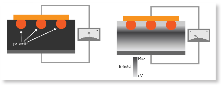 Fig. 2 — In a junction SBD, the peak electric field that occurs under reverse bias is moved away from the metal-semiconductor interface, enhancing reliability.
The junction design is used widely in commercial diodes and has been further refined in merged pin configurations which have relatively higher forward current carrying capacity. Trench structures can also be adopted to boost SBD performance (see figure 3). These are typically associated with improved reverse characteristics including reduced current leakage.
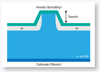 Fig. 3 — Trench structured SBDs are associated with improved reverse characteristics relative to planar configurations.
Superjunction SBD configurations further exploit the potential of SiC diodes to combine high breakdown voltage with low on-resistance (see figure 4). This design shares the submerged p-well structure of the junction configuration but here the well is back-filled with a gate oxide – SiO2. Breakdown voltages of 1350V have been demonstrated combined with an on resistance of just 0.32 mΩ.cm2.
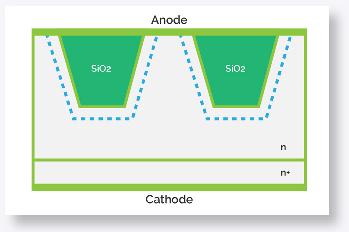 Fig. 4 — A superjunction SBD design further exploits the potential of SiC to deliver a high breakdown voltage in combination with very low on-resistance.
MOSFET
A planar MOSFET structure is shown in figure 5 with Gate (G), Source (S) and Drain (D) terminals. The application of a gate voltage results in the formation of a conducting channel which allows current to flow from source to drain. In the absence of such a voltage the device prevents current flow. It therefore functions as a voltage operated switch. As with the SBD critical characteristics of the device include breakdown voltage and the resistance of the device when current flows - RDS(ON) – which impacts heat generation/power loss.
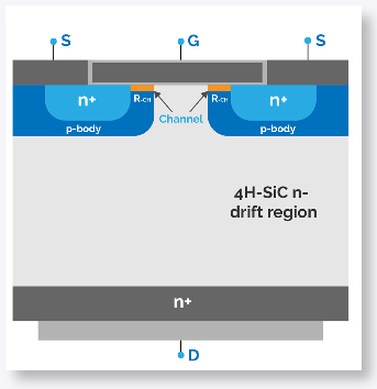 Fig. 5 — A planar MOSFET structure showing contributions to on resistance which is higher than in comparable trench configurations.
MOSFETs can either be manufactured with a planar (figure 5) or trench structure (figure 6) with the gate embedded in the p and n+ layers. A trench structure reduces on resistance by eliminating the JFET region and can therefore offer enhanced performance. However, the likelihood of gate breakdown, which has been a significant problem in the commercialisation of reliable SiC MOSFETs, can be greater, particularly at the base of the trench. In addition, the planar layout can be easier to manufacture.
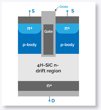 Fig. 6 — A trench MOSFET layout reduces on resistance relative to a comparable planar configuration but can be more prone to gate breakdown.
JFET
JFETs are closely comparable in many respects to MOSFETs (see figure 7) and are likewise voltage controlled. When a voltage is applied across the gate the channel that conducts current from source to drain is 'pinched' or completely switched off. Of the two devices MOSFETs tend to be preferred because they draw less current during use (high input impedance) and consequently have a very low power requirement. Also JFETs operate as normally on which can be a disadvantage in certain applications. Set against this, JFETs have the advantage of being more robust, and importantly for SiC devices, have a configuration that avoids the potential for gate breakdown.
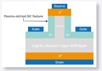 Fig. 7 — SiC JFETs offer some notable attractions but are currently less industrially popular than MOSFETs.
BJT
One further SiC transistor type that has been commercially realised is the BJT (see figure 8), a current as opposed to a voltage controlled device. Current flow between the collector and emitter is controlled by a smaller current flowing between the base and the emitter, with no flow through the base switching off the larger current flow.
Unlike both MOSFETs and JFETs, BJTs are minority carrier devices – both electrons and electron holes are involved in device operation – a characteristic associated with slower switching. On the other hand, BJTs, like JFETs, avoid gate breakdown issues and can have attractive on characteristics, particularly on-resistance which can be low. SiC BJTs have the potential to address many of the limitations of Si BJTs though the fit to industrial requirements has not yet proven sufficiently compelling to drive substantial commercialisation relative to MOSFETs.
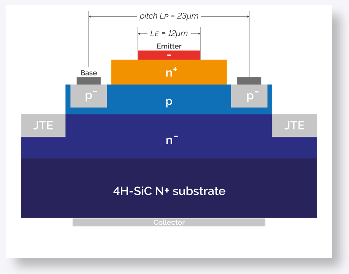 Fig. 8 — Though slower than JFETs and MOSFETs and not in widespread industrial use, SiC BJTs offer low on resistance.
Manufacturing SiC Power Devices
While SiC has attractive properties from the perspective of power device performance, the converse is true with regards to its utility as a manufacturing material. Second only to diamond in terms of hardness, SiC is chemically inert with a high binding energy and exists in as many as 200 different polytypes, crystal structures that are identical in two dimensions but differ in the third.
Polytypes have different properties with 4H the preferred form of SiC for power device manufacture. Maintaining polytype consistency is an important issue in wafer manufacture, which is also complicated by the ease with which defects form – particularly micropipes. As control of crystal manufacturing improves, defect levels are falling, and this is crucial – for the realisation of larger substrate manufacture (150 mm is the current focus) and for certain power devices such as MOSFETs.
From the starting point of a substrate wafer of appropriate quality a broad range of technologies are involved in the manufacture of SiC power devices. Processing steps may include some or all of the following:
- Substrate buffer technology: Buffer layers may be incorporated to tackle defects in the substrate which can penetrate into the epitaxial layer and impact device performance.
- Ion implantation: The diffusion doping of SiC requires extremely high temperatures because of the low atomic mobility of dopants. Ion implantation is preferable and enables precise depth control. However, high ion energies are required and the process can lead to inactive dopants and/or lattice damage which is associated with a requirement for high temperature annealing.
- High temperature annealing: Temperatures required for SiC annealing are typically in excess of 1200°C with temperatures as high as 2000°C routinely required.
- SiC isolation: The oxidation of SiC is used to form gate dielectrics in MOSFETs and for surface passivation.
- Ohmic and Schottky contact formation: This is achieved via sputtered and evaporated metal deposition.
- Edge termination: This is a particular requirement for high voltage devices to prevent voltage breakdown at the edge of a device where field crowding/concentration at junction corners can promote device breakdown. Floating field ring configurations and junction termination extension are the most common strategies deployed for SiC devices but field plates, mesa and bevel structures may also be deployed.
With regards to the contribution of plasma processing, both etching and deposition technologies are required. Plasma etching is used for surface quality improvements prior to epi, mesa formation, potentially in planar devices for edge termination, and for trench formation, while plasma enhanced chemical vapour deposition (PECVD) and/or atomic layer deposition (ALD) are deployed for gate oxide deposition and potentially for the application of a final passivation layer. Figure 9 shows a typical process for the production of a SiC MOSFET with the plasma processing steps highlighted.
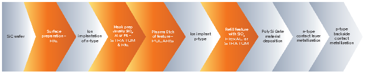 Fig. 9 — The production of a SiC MOSFET is a multistep process in which plasma processing plays a critical role (highlighted in orange).
SiC Etching
The etching of SiC is a key step in the production of almost all of the devices outlined. It is first used to improve the surface of the substrate prior to the epitaxial growth of the device layers. Wafer preparation can introduce defects in the surface at a crystallographic level; if this were to remain in place the device layers would contain unacceptable levels of defects. Plasma etching is used to improve the surface and ensure higher quality layers are grown. Etching is also used to etch features required for the devices, particularly the trench SBD/MOSFET configurations and the superjunction SBD. Figure 10 shows examples of etched features in a trench MOSFET and in a JFET.
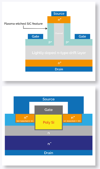 Fig. 10 — Etched features are critical in the manufacture of SiC power devices.
Requirements and Challenges
The development of SiC power device features requires the ability to etch trenches up to 20µm in depth. Edge profile and surface roughness control is critical. Surface roughness, and more specifically micro-trenches, is associated with lower breakdown voltage and increased leakage current. It can also lead to the concentration of electric fields which can exacerbate gate oxide breakdown. The aim is smooth side walls and a level trench base (figure 11).
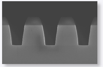 Fig. 11 — Micro-trenching can impact device performance and must be avoided during the etching process.
These requirements, in combination with the physical properties of SiC, set the challenges associated with the etching step for SiC power devices which include:
- Attainment of a commercially viable etch rate: Higher etch rates are directly associated with increased throughput.
- Precision control of trench geometry: To deliver the required device performance, including the precise control of surface roughness/micro-trenching and trench angle.
- Optimisation of selectivity relative to the mask: Poor selectivity necessitates the use of thicker masks which are associated with higher fabrication costs.
Processing Solutions
RIE or more precisely Inductively Coupled Plasma enhanced RIE (ICP-RIE) is the process of choice for SiC etching. RIE involves directional plasma etching and can be used for a wide range of materials. The use of an ICP enhances process performance by enabling the independent control of ion density (RF power to the coil) and ion energy (RF power to the table); RIE has a simpler set-up with a single RF source controlling both parameters. This enhanced functionality means that with ICP-RIE ion density can be tuned to maximise etch rate while ion energy is minimised to reduce substrate damage and enhance selectivity. Figure 12 shows a schematic of an ICP-RIE unit.
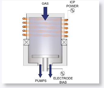 Fig. 12 — ICP-RIE delivers high etch rates, with high selectivity and minimal substrate damage.
Additional benefits of ICP-RIE are that higher plasma density can be achieved at lower pressure enabling better control over selectivity, more directional etching, and better profiles. Furthermore modern systems offer wafer clamping and helium cooling as standard, affording excellent temperature control over a wide operating range and the precise control of device features. With the right plasma chemistry and mask, ICP-RIE is extremely suitable for SiC etching, for power device manufacture.
Example 1: SiC Etching with a SiO2 Mask
Figure 13 shows images of SiC etched features produced through the application of ICP-RIE (Polaris ICP system, Oxford Instruments). Etching was carried out with a SiO2 mask, a standard choice for SiC etching, using SF6/O2 plasma chemistry. This relatively clean chemistry produces etching species with good volatility, a primary requirement for precise feature control.
The etched trenches are of excellent quality with smooth, flat bases and no evidence of micro-trenching. The profile is the required ~86° and the walls are extremely smooth. The etch rate achieved was ~700nm/min which is relatively high for SiC applications and uniformity across the wafer is in excess of +/- 2.2%. Selectivity to SiO2 was in the order of 2.1:1 highlighting the issue of mask selectivity. These levels of selectivity call for a relatively thick mask or suggest the use of alternative conditions and/or masking materials.
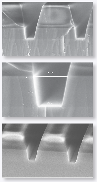 Fig. 13 — Optimised ICP-RIE can deliver precision-controlled SiC features at a commercially viable rate.
Example 2: Low Rate Etch for Damage Critical Applications
A much lower etch rate of ~50nm/min was used to produce the features shown in figure 14 to enable extremely precise control of the etch and minimise any potential for associated damage. This etching was carried out using Cobra ICP system with a SiO2 mask, as in the previous example. The observed selectivity is similar and the profiles produced are of comparable, excellent quality, this time with the required right angled, vertical profile.
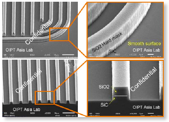 Fig. 14 — A lower etch rate can be preferable when it comes to damage critical applications.
Example 3: Etching with an Al Mask
In this example an Al mask has been applied over the SiO2 mask required for ion implantation with the aim of providing better mask selectivity during the etch step (see figure 15). The etching itself was carried out using the Polaris ICP system. The selectivity to Al is more than double the selectivity to SiO2 observed in the preceding examples – around 5:1 – and the quality of the resulting etches is directly comparable. Smooth 87 – 88° profiles with no micro-trenches and an aspect ratio of more than 5:1 are produced at an etch rate of around 250 nm/min. Uniformity is <+/-5% across a 100 mm wafer.
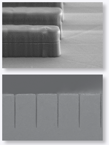 Fig. 15 — A metal mask provides better selectivity during SiC etching, shown here simultaneously protecting a SiO2 mask for ion implantation.
High aspect ratio (HAR) etch processes (figure 16) are especially applicable to superjunction SBD; the deep HAR trench is used to evenly distribute the field and allow for higher breakdown voltage and lower Ron.
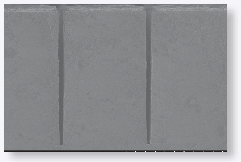 Fig. 16 — HAR etch feature typically used for superjunction SBD devices.
Example 4: Etching with an SU8 Mask
In this example the mask material has been chosen not on the basis of selectivity but for ease of use. SU8 is a widely used epoxy-based photoresist and therefore readily applied. The observed selectivity of the process which was carried out using the Cobra ICP system is relatively low (0.55:1) but this is less critical given the mask material. Etch rate - 300nm/min - and the quality of the resulting features are good (see figure 17). There is no evidence of micro-trenching and the trenches, which are >10µm in depth, have a smooth profile with the required angle of 83°. Uniformity across a 50mm wafer was <+/- 3%.
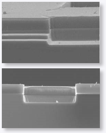 Fig. 17 — SU8 is an easy to use masking material and enables the etching of >10µm trenches at a rate of 300 nm/min.
Gate Oxide Deposition
In a MOSFET the dielectric gate oxide layer separates the gate terminal from the source and drain, and the conductive channel (between S and D) when the device is on. Gate oxide is also used for backfilling applications, as illustrated by the superjunction SBD design. The deposition of high quality gate oxide films is consequently a critical step in the manufacture of many SiC devices.
Requirements and Challenges
SiO2 is the conventional gate oxide for SiC power devices, as with Si, but there are inherent limitations associated with its use, particularly within SiC MOSFETs where gate breakdown has been a major source of reliability concerns due to the high electric fields associated with device operation. Though early gate oxide failure in Si devices has been successfully linked with localised thinning due to contamination during the manufacturing process this mechanism has been discounted for the failure patterns observed with SiC. Rather breakdown has been associated with the relatively high densities of defects in the SiO2 layer.
SiO2 has a low dielectric constant, ~2.5 times lower than that of SiC, and interfaces poorly with SiC. As a result, gate oxide grown on SiC has a much higher density of defects (Dit) than that grown on Si. Proposed mechanisms for SiC gate oxide breakdown suggest that these defects act as electron traps, giving rise to trap assisted tunnelling which in combination with the high electric field stress imposed during use results in locally enhanced leakage currents. The net result is a reduction in the time taken to accumulate the charge associated with breakdown. The types of traps identified include: dangling bonds, carbon clusters at the gate oxide interface, and near interface traps associated with oxygen vacancy defects.
Two different approaches can be adopted to enhance gate oxide performance. One is to improve the quality of SiO2 films through alternative processing solutions such as high temperature annealing in an oxygen containing atmosphere. The second is to use gate oxides with a higher dielectric constant that are inherently more suitable for the application. Here, Al2O3 is one of the primary materials of interest. With a high dielectric constant, a lattice well-matched to that of SiC, good thermal stability and additional beneficial electrical properties Al2O3 has potential either alone or layered with SiO2.
Whichever approach is taken the requirement is for high quality films free of crystals and other bulk defects potentially deposited at relatively high aspect ratios; designs such as the trench MOSFET designs may require HARs >5:1.
Processing Solutions (1): PECVD
PECVD is the simplest and fastest technique for gate oxide deposition and is particularly suitable for SiO2. In PECVD a film is formed via the reaction and deposition of ionised gases from a plasma on a cooled substrate. Figure 18 shows a schematic of a PECVD unit.
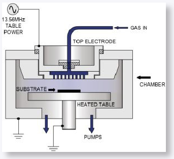 Fig. 18 — PECVD enables the deposition of high quality SiO2 films at relatively low working temperatures.
Radicals and ions from a plasma generated by the application of RF at the top electrode form a film on the substrate surface; unwanted reaction by-products are pumped away. PECVD is a flexible process that can be used for an extremely wide range of materials. It produces highly uniform, high density films with minimal pinholing/defects at relatively modest operating temperatures, with tetraethylorthosilicate (TEOS) chemistry particularly useful for SiO2 step coverage.
Example 5: Using PECVD for Gate Oxide Deposition
Table 3 summarises the performance characteristics of SiO2 PECVD with a typical processing unit (Stratum PECVD, Oxford Instruments). N2O/SiH4 plasma chemistry was used here which is a combination which produces high quality films. Wet etch rates quantify the quality of the film, lower rates being indicative of higher quality. However, in this instance the more relevant metric for film quality is breakdown voltage which was found to be in the order of 7MV/cm with an associated leakage current (at breakdown) of 6.41*10-9 A/cm2. These data are for a deposited film of 110nm thickness.
| Film Property |
Results |
| Deposition rate |
50nm/min to >1200nm/min |
| Film thickness uniformity (200mm, 38pt, 10mm edge exclusion) |
<±3% |
| Refractive index |
1.46–1.48 |
| Film Stress |
<-100MPa (compressive) |
| Wet etch rate (BHF 10:1, 20°C) |
<200nm/min (achieved ~120nm/min) |
Table 3: PECVD can deposit high quality SiO2 films at a relatively fast rate.
Figure 19 shows a uniform PECVD film covering an open feature. Though PECVD is an efficient technique for low aspect ratio features, at higher aspect ratios it can deliver poor conformality. Where this is an issue ALD may be preferred for gate oxide deposition.
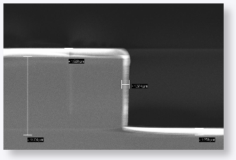 Fig. 19 — PECVD is an efficient technique for the deposition of high quality films at relatively low aspect ratios but higher aspect ratios may be better served by ALD.
Processing Solutions (2): ALD
ALD is a process with two defining characteristics: self-limiting atomic layer-by-layer growth and highly conformal film growth. The key features of an ALD unit are shown in figure 20.
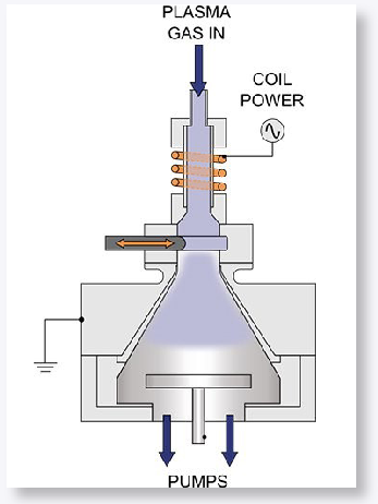 Fig. 20 — ALD enables the precision deposition of high quality films, even at high aspect ratios, for a wide range of materials.
The layer-by-layer growth delivered by ALD is a result of a cyclical sequence of plasma pulses followed by associated purge steps. The first plasma pulse results in the absorption and reaction of a gaseous precursor onto the surface of the substrate, leaving a single monolayer. The following purge removes unwanted reaction by-products along with any unabsorbed precursor. A second plasma pulse provides a further reactant, to complete the deposited layer, and is followed by a further purge. Repeating these sequences progressively builds the coating or film which can consequently be produced both pin-hole and particle free.
The high conformality of the technique, an important advantage in many applications, stems directly from this mechanism of film growth which restricts reaction at the surface to no more than a single layer of precursor. ALD is also prized for its ability to coat high aspect ratios. This is achieved through the use of relatively long pulse times which enable the precursors to penetrate deep into a trench to completely coat its surface. In combination these features make ALD an attractive choice where gate oxide requirements are especially demanding and there is a need for high quality, high dielectric constant films with good conformality. ALD is the technique of choice for Al2O3 deposition, because the temperatures associated with the use of PECVD for this material tend to be relatively high, eroding any potential benefit. It can however be a relatively slow process so other deposition technologies may be preferable if film quality is acceptable.
Example 6: Using ALD for SiO2 Deposition
Figure 21 shows images of a SiO2 layered feature on a Si device, manufactured by ALD (FlexAL ALD Tool, Oxford Instruments). The resulting film is around 100nm thick and has excellent quality, as evidenced from its breakdown voltage which is in excess of 10MV/cm at 200°C (see table 4). The film has excellent conformality even though the aspect ratio (AR) is very high but deposition rate - 1.3 nm/min – is far slower than the rate achieved with PECVD.
| High rate SiO2 PEALD process |
|
| VBD |
>10MV/cm at 200°C dep temp |
| Cycle time (PEALD) |
1.3nm/min |
| Thickness uniformity (200mm, 3mm EE) |
<±2.6% |
| Thickness repeatability |
<±1.6% |
| Conformality |
>90% >30:1 AR substrate at 300°C deposition temperature |
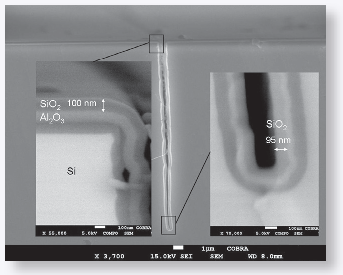 Fig. 21 — ALD delivers higher quality films than PECVD, with excellent conformality, but at lower deposition rates.
Conclusion
While SiC has excellent properties from the perspective of power device performance it presents manufacturers with significant challenges. Realising the potential of SiC to deliver power devices that are smaller, lighter, more efficient and closely tailored to pressing industrial requirements relies on developing manufacturing protocols that can robustly realise a range of configurations. Plasma processing has a key role to play with both etching and deposition technologies vital to the manufacturing process. In this white paper we highlight the tools that are available and the performance that can be delivered, illustrating how plasma processing techniques can be used to cost-effectively access the breakthrough power device performance that SiC offers.
References
- S. Saddow et al. 'Advances in Silicon Carbide Processing and Applications' Artech House 2004
- X. Zhong et al. 'Design and Experimental Demonstration of a 1.35kV SiC Super Junction Schottky Diode' Proceedings of the 2016 28th International Symposium on Power Semiconductor Devices and ICs (ISPSD) June 12–16, 2016, Prague, Czech Republic
- M. Baudelot 'SiC Power Devices' Dec 2009
- X. She 'Review of Silicon Carbide Power Devices and their Applications' IEEE Transactions on Industrial Electronics, Vol 64, No 10, Oct 2017
- 'JFET vs. MOSFET' Learning about Electronics
- W. Bergner et al. 'Infineon's 1200V SiC JFET – The New Way of Efficient and Reliable High Voltage Switching'
- S. Araujo et al. 'Resurrecting the BJT: new SiC BJTs enable lower system cost in a PV inverter' Electronic Product Design and Test, 5th Feb 2013
- Z. Chbili et al. 'Modelling early breakdown failures of gate oxide in SiC power MOSFETS' IEEE Transactions on electron devices, Vol 63, No 9, Sept 2016
- T. Gutt et al. 'PECVD and Thermal Gate Oxides on 3C vs. 4H SiC: Impact on Leakage, Traps and Energy Offsets' ECS Journal of Solid State Science and Technology, 4 (9) M60–M63, 2015
- M. Nawaz 'On the evaluation of gate dielectrics for 4H-SiC based power MOSFETs' Active and Passive Electronic Components, Vol 2015
- R. W. Johnson et al. 'A brief review of atomic layer deposition: from fundamentals to applications' Materials Today, Volume 17, Number 5, June 2014

