Understanding Precipitates and Grain Boundary Composition at the Nanoscale
Many modern alloys rely on nanoscale precipitates and controlling subtle compositional gradients at grain boundaries to achieve their desired mechanical properties and corrosion resistance. Understanding these features requires analytical techniques capable of detecting small chemistry variations at sub-micron spatial resolutions. Traditionally, this presents a challenge for SEM-EDS workflows; Improving spatial resolution requires lower accelerating voltages, but lower voltages significantly reduce X-ray generation and increase acquisition times.
This application note demonstrates how the backscattered electron and X-ray (BEX) technique can maintain high analytical speeds at reduced current and voltage, allowing users to rapidly characterise sub-micron features that would otherwise require lengthy EDS acquisitions.
The Speed and Spatial Resolution Trade-off
The spatial resolution of SEM-EDS is determined by the electron beam interaction volume, the three-dimensional region of the sample in which the primary electron beam can generate X-rays (Fig. 1). The size of this interaction volume depends on two factors: (1) the beam accelerating voltage and (2) the average atomic number of the sample. Therefore, for any given sample, improved SEM-EDS spatial resolution can be achieved by lowering the accelerating voltage.
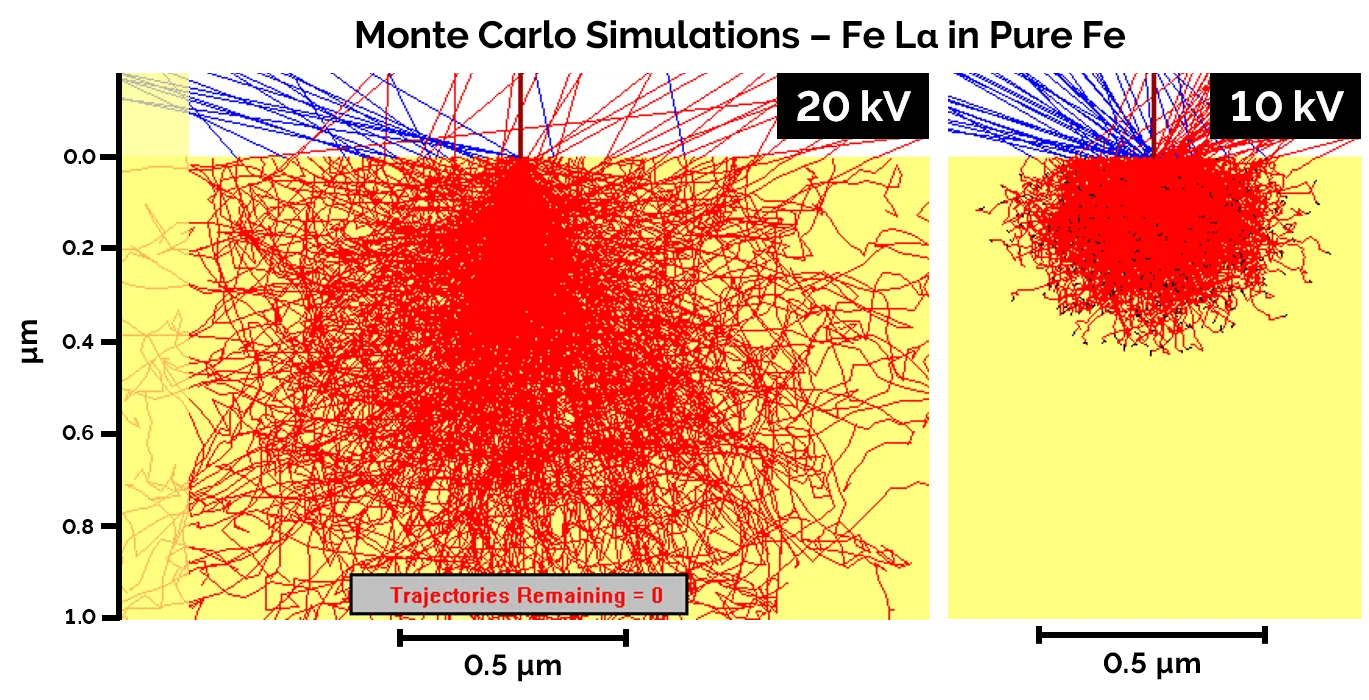 Figure 1. Monte Carlo simulations of Fe Lα X-ray production in bulk Fe, shown on a unified 0.1 µm grid with independently normalised density scales for 20, 15 and 10 kV accelerating voltages.
However, as the accelerating voltage is reduced, the probability of generating X-rays decreases substantially. Consequently, lower-voltage SEM-EDS produces lower count rates and requires longer acquisition times.
This effect was demonstrated on a pure Fe standard using simultaneous EDS and BEX at varying accelerating voltages (Fig. 2). As voltage decreased, Fe Kα peak area fell sharply for both techniques. However, between 10 and 15 kV, BEX collected 3–10 times more X-rays than conventional EDS, regardless of whether EDS was performed using Fe Kα or the lower-energy Fe Lα line (Fig. 2B). This higher count rate comes from the BEX detectors position beneath the pole piece, closer to where X-rays are generated.
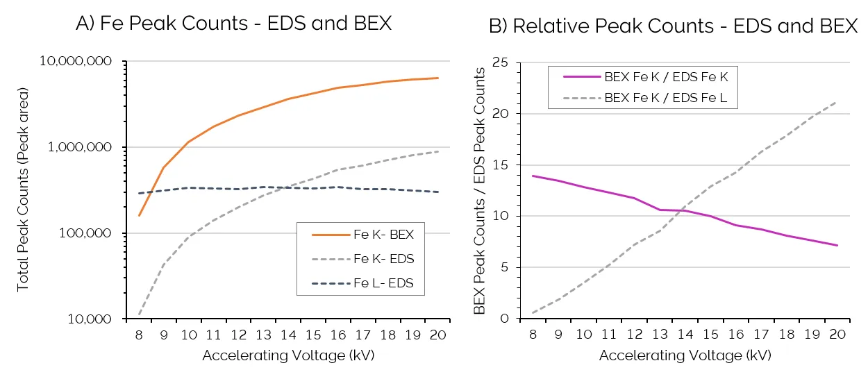 Figure 2. (A) Fe peak counts, measured as peak area for K and L lines, collected during analysis of an Fe standard using EDS and BEX at different accelerating voltages. B) Relative peak area of BEX and EDS detectors (BEX peak are / EDS peak area). All analyses were performed at a working distance of 8.5 mm, beam current of 1.95 nA, and live time of 10 s. EDS data were collected using an Ultim Max ∞ 100 at process time 2.
What Does All This Mean?
The peak area test shown above highlights a major data collection advantage. For X-ray mapping of metallic particles in the 0.2-1 µm size range at 10 to 15 kV, a system equipped with BEX collects 3 to 10 times more data than a large 100 mm2 EDS detector. This massive increase in signal is achieved in the exact same acquisition time under identical beam conditions. In practical terms, an Fe-Kα map that would require 10 minutes using a 100 mm2 EDS could be reduced to as little as 1 minute with BEX.
Understanding Alloy Structure at the Nanoscale
In high-strength 7000-series aluminium alloys (Al-Zn-Mg-Cu), mechanical performance and corrosion resistance are governed by the size, distribution and chemistry of inclusions and precipitates formed during solidification, heat treatment and ageing. Solidification first produces coarse intermetallic particles, whilst during ageing, Zn- and Mg-rich precipitates form in the matrix and at grain boundaries. At grain-boundaries, such precipitation can consume the nearby solutes (Mg, Cu, Zn), generating solute-depleted zones (SDZs) which promote corrosion.
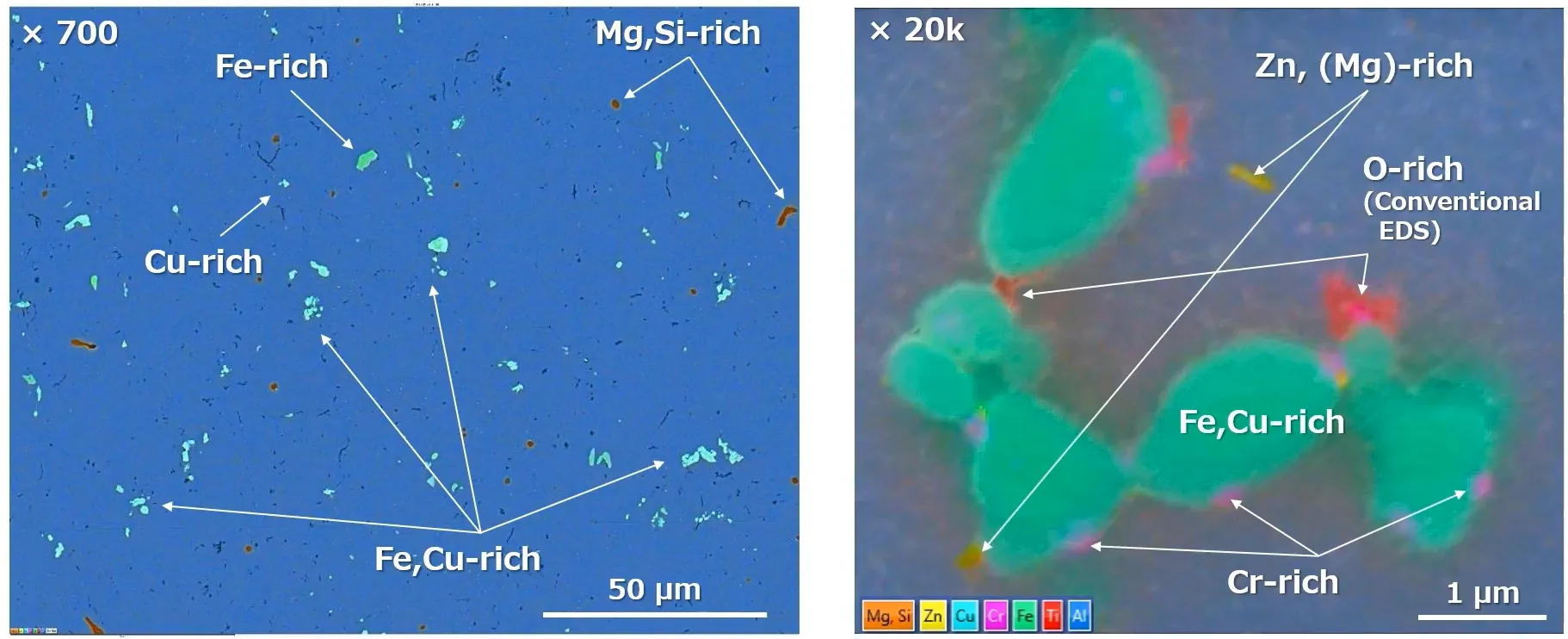 Figure 3. BEX images of diverse aluminium alloy precipitates on the micro and nanoscale
In this application example performed on a FEG SEM by JFE Techno Research, these critical intermetallic phases, precipitates and grain boundary depletion zones are easily visualised within the BEX dataset (Fig. 3 & 4). These include micron scale Mg, Si, and Fe phases alongside nanoscale Cu and Zn rich precipitates that form at the grain boundaries and are surrounded by SDZ’s. Compared with conventional EDS (Fig. 4), the grain-boundary precipitates and SDZ are resolved with far greater clarity owing to the enhanced sensitivity of the BEX technique to Cu Kα and Zn Kα X-rays. Because Cu and Zn depletion at grain boundaries drastically reduces corrosion resistance, the ability to rapidly SDZs means JFE can now identify critical microstructural evolution with unprecedented turnaround. This enables a significantly faster time to insight for process optimization using an accessible tool available on SEM platforms.
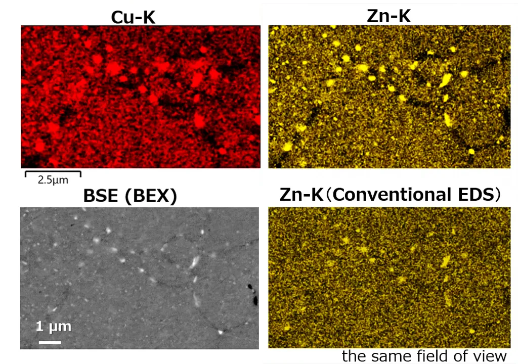
Figure 4. BEX X-ray maps and BSE image of grain boundaries and precipitates with simultaneously acquired EDS Zn X-ray map.
Conclusion: Characterising Alloy Microstructure with Greater Efficiency
The inclusions, precipitates and grain-boundaries that control alloy corrosion resistance and mechanical performance require reduced accelerating voltages to allow elemental characterisation on the nanoscale. However, X-ray counts fall under such conditions, leading to lengthy acquisition times and longer timescales for process optimisation. Unity BEX addresses this trade-off by placing X-ray sensors beneath the pole piece, closer to where X-rays are generated. This geometry captures more signal under the same beam conditions, giving faster assessment of sub-micron features that drive material performance.

