Introduction
Transmission Kikuchi diffraction (TKD) is a relatively recent development in EBSD that allows high resolution analysis of electron transparent samples. Most applications in the literature have used TKD for targeted measurements of relatively small areas, on samples where conventional EBSD struggles to deliver the required resolution [1]. These samples are typically nanocrystalline metals and alloys, although increasingly the technique is also being used to characterise highly deformed samples, where the high dislocation density makes characterisation using conventional EBSD very challenging.
In this application note we look at a range of sample types, including severely deformed Al-alloys and steels as well as an electrodeposited, nanocrystalline Ni. The TKD analysis results show how the sensitivity and speed of Symmetry can provide significant benefits in these high-end applications.
Materials and Methodology
Four different samples were analysed in this study:
- Equal channel angular pressing (ECAP) deformed Al-Sc alloy
- ECAP-deformed Al-Mg-Cu alloy
- High pressure torsion (HPT) deformed steel
- Electrodeposited nanocrystalline Ni
All of the samples were prepared by electropolishing 3 mm diameter TEM discs until a perforation was observed in the centre. TKD measurements were carried out in a FEG SEM using an accelerating voltage of 30 kV, with samples mounted at a short working distance in a horizontal position.
The diffraction patterns were collected using Symmetry operating at various resolutions, with measurement parameters as shown in Table 1. The final orientation maps were processed to remove non-indexed points along some boundaries and a few misindexed pixels.
| Sample | Scan size | Step size | Speed | Pattern resolution | Hit rate |
| ECAP Al-Sc* | 2263 x 2407 | 50 nm | 974 pps | 156 x 128 | > 90 % |
| ECAP Al-Cu-Mg | 600 x 600 | 10 nm | 100 pps | 622 x 512 | ~ 88 % |
| 1569 x 2782 | 1569 x 2782 | 8 nm | 100 pps | 311 x 256 | ~ 83 % |
| HPT steel | 249 x 273 | 4 nm | 165 pps | 311 x 256 | ~ 80 % |
| Nano Ni | 250 x 268 | 2 nm | 125 pps | 311 x 256 | ~ 80 % |
Table 1. Analysis parameters used for the TKD measurements in this study.
* This was an elliptical area including the perforation; hit rate is an estimate on the Al sample itself.
Results
The resulting orientation map of the large scan of the Al-Sc alloy is shown in Fig. 1. This highly deformed alloy has been effectively characterised on a large scale: the total analysis took only 45 minutes at close to 1000 indexed patterns per second. This overview map is ideal for surveying the whole TEM sample in order to identify areas of interest for subsequent higher resolution analyses, either using TKD or in the TEM. The Symmetry detector and algorithms within AZtec enable reliable indexing from the edge of the perforation right across to significantly thicker areas of the sample: this would not be possible with a so-called on-axis TKD geometry, which is much more sensitive to thickness variations.
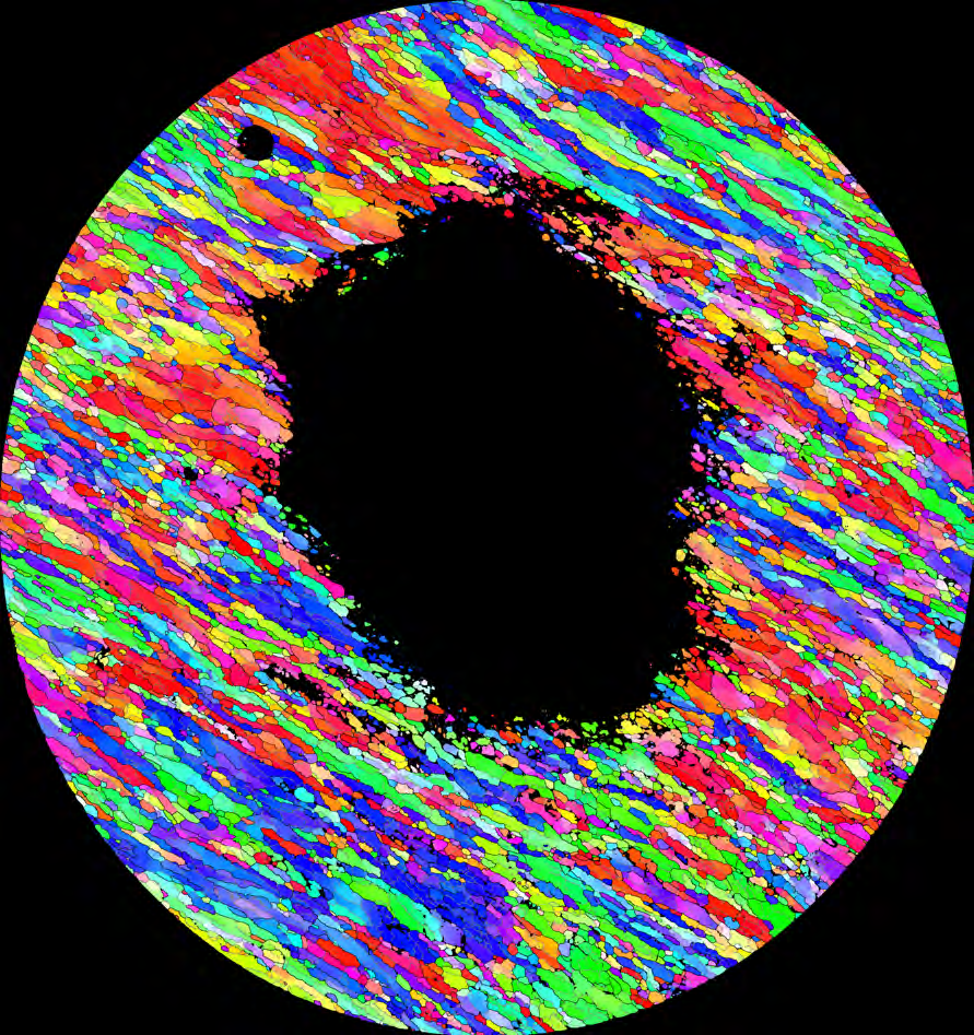
Fig. 1. Overview TKD scan around the perforation in a TEM sample from an ECAP deformed Al-Sc alloy. IPF colouring scheme.
In the second deformed Al-alloy, the ECAP deformation has resulted in ultrafine-grained shear bands that are impossible to analyse effectively using conventional EBSD. A 6 x 6 μm area within one such shear band was scanned in approximately one hour, and the final pattern quality and orientation maps are shown in figure 2. The presence of many nanostructured grains, under 100 nm diameter, is clear but there are also numerous elongate grains several μm long. These are highly substructured, with numerous low angle boundaries and regions of more diffuse local misorientation. Even so, the mean grain diameter in this area is 170 ± 5 nm.
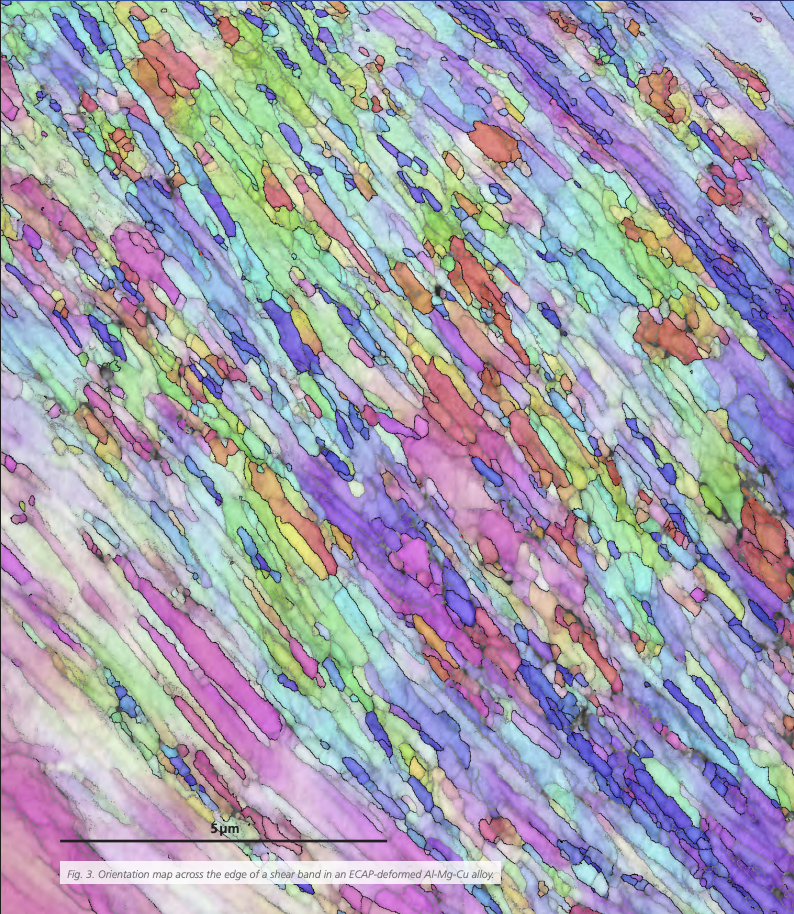
The second, larger analysis on this sample examined the edge of one of the shear bands (Fig. 3): here the grain size refinement had not continued to the same extent as shown in Fig. 2, with many more elongate, larger grains remaining. The results show how larger area TKD analyses are often required in order to characterise effectively heterogeneous microstructures such as in this alloy.
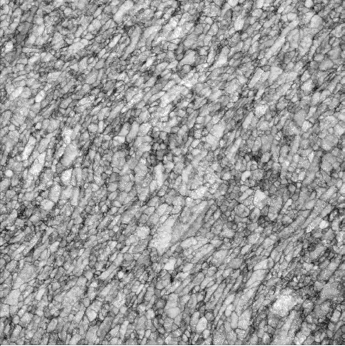
Fig. 2a. Pattern quality map of an ECAP deformed Al-Mg-Cu alloy.
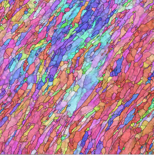
Fig. 2b. Orientation map of the same area, with high angle boundaries in black, low angle boundaries in grey
The steel sample, deformed at room temperature using HPT, has a more nanostructured microstructure, as shown in Fig. 4. The mean grain diameter here is 51 ± 2 nm, and it can be seen that the TKD analysis has resolved all but the very finest grained regions. In addition to the nanostructured grain size, many of the grains in this sample contain significant densities of geometrically necessary dislocations (in the 1016 m-2 range), resulting in orientation changes exceeding 10° across 100 nm transects. There are also a few grains that contain Σ3 twin boundaries (red lines in figure 4b), an interesting observation in a ferritic sample. The ability of Symmetry to collect EBSPs quickly and with good resolution (in this case 311 x 256 pixels at 165 pps) has enabled an effective and quick characterisation of this very challenging microstructure.
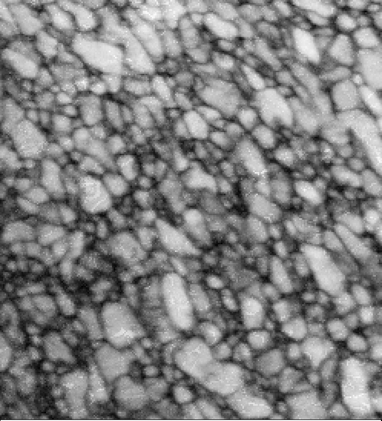
Fig. 4a. Pattern quality map of an HPT-deformed steel sample.
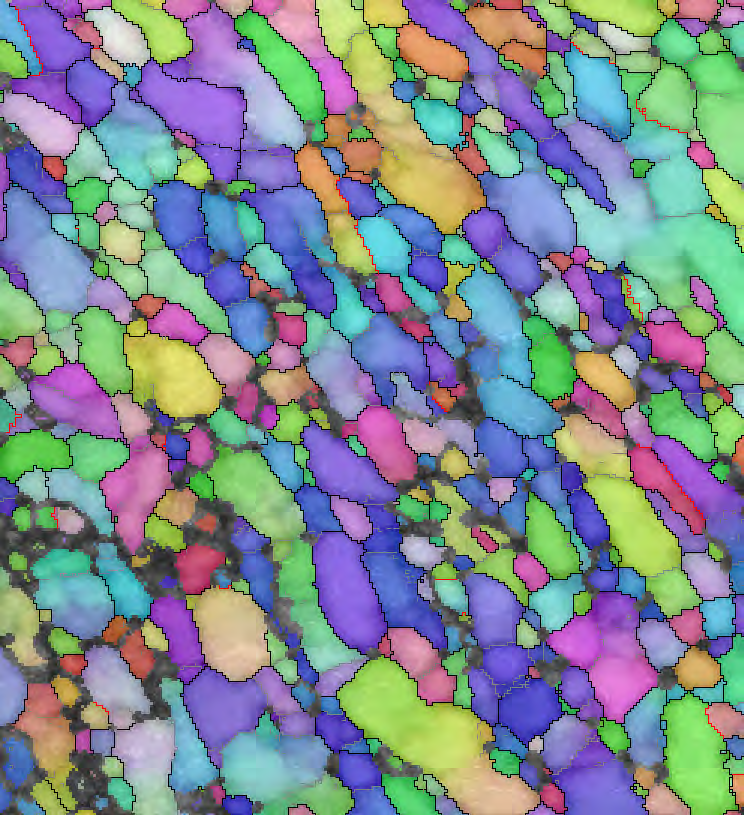
Fig. 4b. Orientation map (IPF colouring) of the same area, with high angle boundaries in black, low angle boundaries in grey and Σ3 twin boundaries in red.
The final sample analysed in this study is an example of a bottom-up approach to forming nanocrystalline material. Rather than refining an originally coarse grained material using severe plastic deformation, this sample has been electrodeposited with a nanocrystalline structure from the start. The challenge for analysis here is the exceptionally fine grain size – significantly less than 50 nm. The pattern quality and grain size maps shown in Fig. 5 illustrate that TKD, with a measurement step size of 2 nm, is able to characterise effectively this nanostructured sample. Many of the grains contain Σ3 twin boundaries (shown in red in Fig. 5b) but even disregarding these boundaries, the majority of grains have a diameter under 50 nm and many are less than 20 nm (blue in Fig. 5b). The mean grain size of this sample is 20.8 ± 0.5 nm, based on more than 500 measured grains.
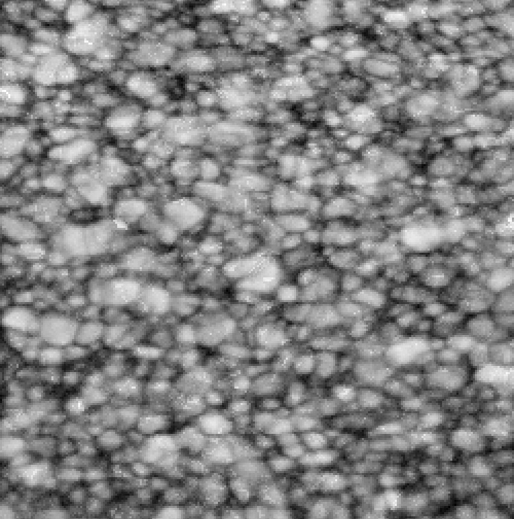
Fig. 5a. Pattern quality map of a nanocrystalline Ni sample
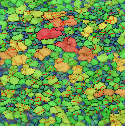
Fig. 5b. Grain size map of the same area. Note that blue grains have a diameter under 20nm. Twin boundaries (red lines) have been excluded from the grain size measurement.
Conclusion
The results shown in this report give a clear indication of the power of the CMOS-based Symmetry EBSD detector for effective analysis of nanostructured and severely deformed materials using TKD. The ability to collect good resolution diffraction patterns at high speed, and the sensitivity to optimise the SEM beam conditions without having to compromise on acquisition rates, makes Symmetry the ideal detector for TKD analyses.
In addition, adjusting the phosphor screen elevation using Symmetry's variable tilting mechanism allows users to ensure that the sample and detector are always in the perfect geometry for high resolution TKD analyses. These results illustrate how superfast TKD provides a rapid, detailed overview of whole TEM samples and how, with optimum beam conditions, TKD can be used to characterise samples with a mean grain size as small as 20 nm.
Reference
- Sneddon et al. (2016). Materials Science and Engineering: R: Reports. 110, p 1-12.
Acknowledgments
Oxford Instruments thanks Katja Eder and Adam Sikorski (Australian Centre for Microscopy & Microanalysis) for providing the Al-Sc alloy and assisting with TEM sample preparation.

