GaN-based high-electron-mobility transistors (HEMTs) require accurate, spatially resolved temperature measurements to
assess device thermal behavior and reliability. This Application Note presents thermomechanical Raman mapping of GaN
HEMTs based on Raman thermometry using temperature-induced shifts of the E2(high) phonon mode. Measurements
were performed using a witec360 confocal Raman microscope, enabling non-destructive determination of local temperature
distributions at the microscale.
Introduction
GaN-based High-Electron-Mobility Transistors (HEMTs) surpass conventional silicon microchips in efficiency and
switching speed. In addition, they are significantly smaller than their silicon counterparts and offer superior
thermal resilience.
For manufacturers of highly advanced semiconductor devices, fast and exceptionally accurate metrology is essential.
Spatially resolved thermometry is a key application to understand the electric devices under operating load. The
witec360 confocal Raman microscope provides all key capabilities required to meet these demands. With its outstanding
spatial and spectral resolution, it enables users to investigate material properties non-destructively at a
fundamental level. Its modular design allows the system to be configured precisely to the customer’s application
needs.
In this Application Note, we present a guide to generate thermomechanical Raman maps derived from temperature-induced
peak shifts of the E2(high) Raman phonon mode in a GaN based HEMT.
The investigated sample was provided courtesy of the Nanotechnology Research Center (NANOTAM), Bilkent
University, Turkey.
Confocal Raman setup for GaN HEMT mapping
For these measurements, a fully automated witec360 confocal Raman microscope equipped with a 532 nm excitation laser
was used. TruePower ensured highly accurate and reproducible laser power control, providing an adjustment accuracy of
0.1 mW.
The integrated RayShield filter enabled simultaneous acquisition of both Stokes and anti-Stokes Raman signals, which
allows direct temperature measurement. Raman detection was performed using a Hexalight spectrometer with 300 mm focal
length and an 1800 g/mm diffraction grating. This configuration allowed the simultaneous measurement of the
temperature via Boltzmann-statistics and stress-sensitive E2(high) phonon mode of GaN (~ –567 rel. 1/cm for
anti-Stokes and ~ 567 rel. 1/cm for Stokes) without compromising spectral resolution. Since the anti-Stokes intensity
is inherently weak, especially at temperatures close to ambient conditions, exceptional spectrometer sensitivity is
essential for reliable data acquisition.
For controlled sample heating, an in-house-built temperature stage was employed, covering a range from ambient
conditions up to 200 °C. If extended temperature ranges are required, a Linkam stage can be easily mounted beneath the
objective.
Measurement preparation for Raman thermometry
For high-quality measurements, a well-aligned system is essential. Accurate spectral calibration must therefore be
ensured. The integrated HgAr-calibration light source provides a one-click solution for spectral calibration and
verification based on atomic emission lines. For compliance checks, spectral certification can be performed using a
standard reference sample such as cyclohexane.
In addition, a precisely aligned pinhole is crucial for achieving optimal spatial resolution while maintaining
excellent throughput. AutoBeam technology offers another convenient one-click solution for automated pinhole
alignment.
Accurate measurements require careful sample handling and proper fixation of the specimen on the heating stage. In
this case, the microchip was secured using two leaf springs. To ensure efficient heat transfer from the stage to the
sample, a thin layer of thermal paste was applied.
As a microchip contains numerous micro scale functional units, it is important to obtain an overview of the entire
sample to identify the region of interest (ROI). Therefore, an overview stitching image was recorded using a 5x
objective (Figure 1, left panel). One of the GaN-based HEMT transistors, shown in the center panel, was selected for
detailed investigation. The close-up image (right panel) acquired with a 100x objective highlights the ROI (green
box), which was subsequently analyzed using confocal Raman microscopy.
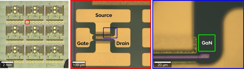
Figure 1: Bright-field images of the microchip and the investigated ROI. The left panel shows a stitched overview
image of the entire microchip. The center panel is a magnified view of the red-boxed region, acquired with a 20x
objective. The right panel provides a further zoom of the blue box, obtained with a 100x objective, and highlights the
investigated ROI (green box).
Raman data acquisition for phonon peak shift analysis
For the first measurement, the temperature of the heating stage was set to 25 °C. An area of 20 x 20 µm2
(Figure 1, right panel, green box) containing the semiconducting GaN was investigated using confocal Raman microscopy.
A spatial resolution of 333 nm/pixel was applied, resulting in 60 x 60 = 3600 recorded pixels. The laser power before
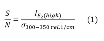
the objective was set to 40.0 mW. A sufficient signal-to-noise ratio of ~ 160 (formula 1) of the E2(high)
mode was achieved with an integration time of 50 ms per pixel. This corresponded to a total measurement duration of 3
minutes and 33 seconds.
After completing the measurement, the heating stage temperature was increased to 40 °C. Since the sample exhibited
thermal drift due to heating, the measurement area was slightly adjusted (approximately a 3 µm offset). The
measurement was then repeated using the same parameters as before. The temperature was increased subsequently to 190
°C in 20 °C steps, and the measurements were performed accordingly.
Spectral analysis and phonon peak fitting
The batch analysis functionality integrated into the Project software was particularly advantageous, as it enabled
the simultaneous processing of all ten acquired Raman image datasets using identical analysis parameters. Data
evaluation was performed using the Raman analysis module, which provides a guided, step-wise workflow for
preprocessing, spectral analysis, and visualization, ensuring consistency and reproducibility across the entire
dataset. After the data evaluation, a statistical analysis of the results was also performed within the Project
software.
The evaluation follows a defined structure, containing cosmic ray removal, background subtraction,
and peak fitting.
Cosmic ray removal is a functionality to get rid easily of effects of cosmic particles like muons and
(secondary) electrons interacting with the CCD.
Background subtraction was performed using the Shape tool. In this method, a rounded baseline is iteratively
fitted beneath each spectrum on a pixel-by-pixel basis and subsequently subtracted. The Shape algorithm is
particularly effective for removing broad fluorescence contributions and is noteworthy for its robustness and ease of
application.
Peak fitting: After background subtraction, the temperature-sensitive position of the GaN
E2(high) phonon mode was determined for all 36.000 acquired spectra (Figure 2). The Raman peak was fitted
using a pseudo-Voigt function, which provides a more accurate representation of the line shape than a purely Gaussian
or Lorentzian function. Acquiring full Raman images yields significantly more robust statistical information compared
to analyzing only a small set of individual spectra per temperature point. The high throughput of the witec360 system,
combined with the newly developed Hexalight spectrometer, enables the acquisition of a large number of spectra in a
very short time, thereby facilitating rapid and comprehensive statistical evaluation.
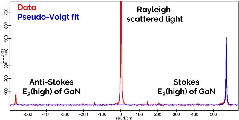
Figure 2: Raman spectrum of GaN recorded at 100 °C. The spectrum shows both the anti-Stokes and Stokes components of
the stress- / strain- and temperature-sensitive GaN E2(high) phonon mode, as well as the elastically
Rayleigh-scattered light. The red curve represents the processed data after cosmic ray removal and background
subtraction, while the blue curve shows the pseudo-Voigt fit applied to the Stokes E2(high) mode.
The final step of the data processing workflow was the statistical evaluation (Figure 3), which was performed
simultaneously for all datasets in a straightforward and efficient manner.
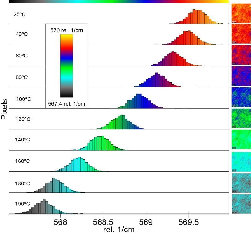
Figure 3: Statistical evaluation of the temperature-sensitive GaN E2(high) phonon mode at different
temperatures. The histogram displays the distribution of the extracted peak positions, while the accompanying images
illustrate the spatially resolved peak position for every recorded spectrum at the respective temperature.
Boltzmann-based Raman thermometry
To determine the temperature of the sample surface, a Boltzmann-based Raman thermometry approach was applied. The
temperature was calculated using formula 2,
where h is Planck’s constant, c is the speed of light, and kB is the Boltzmann constant. IA and
IAS are the intensities (applying a sum-filter) of the Stokes and anti-Stokes components, respectively.
λS and λAS denote the corresponding wavelengths of the Stokes and anti-Stokes
E2(high) phonon modes. ν̃ is the Raman shift of the E2(high) phonon mode, and the averaged value
obtained at room temperature (ν̃ = 569.7 rel. 1/cm) was chosen for all datasets as an approximation. To extract the
required intensities and wavelengths for the Boltzmann-based temperature analysis, average spectra were computed for
each complete dataset. This process was performed in a single step using the integrated functionality of the Project
software.
Thermomechanical Raman map generation
For the computation of the final thermal maps, a calibration curve was required. Therefore, the average values and
standard deviations of the GaN E2(high) peak positions were extracted from the histograms at each
temperature. These averaged peak positions were then plotted as a function of temperature, which was either extracted
from the software (Figure 4) or obtained from the Boltzmann-based approach (Figure 5). Because the E2(high)
phonon mode exhibits an approximately linear dependence on temperature, a linear fit was applied to the data.
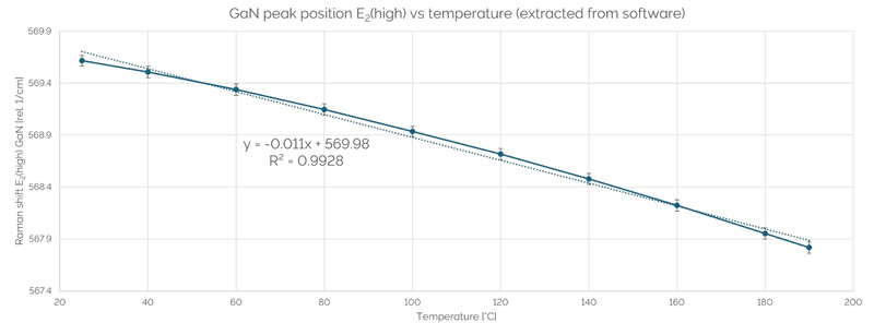
Figure 4: Evaluation of the peak position of the E2(high) mode as a function of the temperature extracted
directly from the software, including the corresponding linear regression (dotted line).
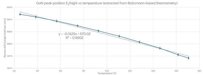
Figure 5: Evaluation of the peak position of the E2(high) mode as a function of the temperature calculated
from Boltzmann-based thermometry, including the corresponding linear regression (dotted line).
While both calibration approaches yielded consistent results, there is a small discrepancy between the temperatures
obtained from the software and the Boltzmann-based Raman thermometry. This can be attributed to heat dissipation and
thermal gradients between the heating stage and the sample surface. The temperature reported by the software
corresponds to the set and measured value of the heating stage, whereas the Boltzmann-based method directly reflects
the local temperature at the sample surface. Therefore, the Boltzmann-derived temperatures were used for generating
the thermal maps, as they provide the most accurate representation of the actual sample surface temperature. One
thermal map is exemplarily shown (Figure 6), the temperature was set to 100 °C in the software.
To generate the thermal maps, the Raman peak shift of the E2(high) mode was inserted into the calibration
obtained from the linear regression. This computation was performed for each pixel of the Raman image using the
built-in calculator functionality of the Project software.
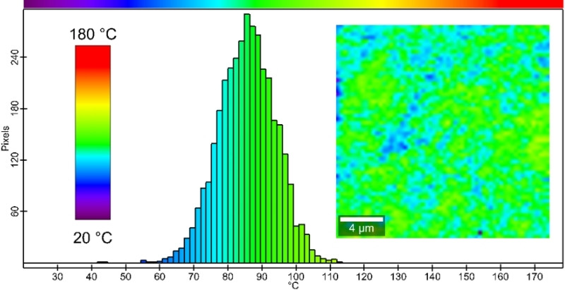
Figure 6: Thermal map of the GaN layer on the HEMT device together with the corresponding temperature distribution
histogram. The temperature set on the software was 100 °C.
Conclusion
In this Application Note, the complete workflow for generating a thermal map of GaN on a HEMT device using confocal
Raman imaging was demonstrated step by step. Raman maps were acquired at different temperatures, and the position of
the GaN E2(high) phonon mode was extracted using a pseudo-Voigt peak fit. The temperature at the sample
surface was independently determined using Boltzmann-based Raman thermometry. All data were acquired with the Control
software, and the entire data evaluation process was performed seamlessly within the Project software environment,
except for a simple linear regression.
This study highlights not only the scientific robustness of the approach but also the remarkable ease of use of the
witec360 system. From rapid data acquisition to automated batch processing and intuitive statistical evaluation, both
hardware and software enable the creation of detailed thermal maps in a straightforward and highly efficient manner.
For future investigations, the GaN HEMT device can be probed under electrical load. Using the Raman shift of the
E2(high) mode, thermal maps of the active device region can be generated with minimal effort. Furthermore,
by incorporating an acousto-optic modulator, Raman measurements can be triggered at defined time intervals after
switching the device on or off. This capability enables time-resolved thermometry, allowing users to study device
heating and cooling kinetics with exceptional simplicity and precision.

