Introduction
Nanoparticles are ubiquitous in the cosmetic and food industries as, among other uses, pigment. Often, nanoparticle mixtures are composed of a single material but with different crystallographic phases. Due to their size distribution and shape, it is difficult to discriminate between phases, but this is necessary for regulatory use. For example, anatase and rutile, polymorphs of TiO₂ are traditionally used in cosmetics, paints, toothpastes, and as food colourants, whereas ferrous oxide nanoparticles are used as food colouring for yellow E172(iii), red E172(ii) and black E172(i).
Various analytical techniques can determine the size and shape of such particles, including Atomic Force Microscopy (AFM), Small-Angle X-ray scattering (SAXS) or Electron Microscopy (EM), but there is a clear need to discriminate between them according to their crystallographic structure [1].
Electron Backscatter Diffraction (EBSD) in the scanning electron microscope (SEM) has the potential to be effective for nanoparticle characterisation, with a high spatial resolution, fast analysis speeds and effective discrimination between different crystal structures. Traditionally, sample preparation for EBSD analysis is a crucial step, since the diffracted signal originates from within tens of nanometres of the specimen surface [2]. This means that any deformation of the sample surface inhibits the ability to acquire data using EBSD. For most materials, the sample must be prepared for EBSD analysis using a final stage of polishing with colloidal silica to achieve a suitable finish.
Conventional EBSD can be used to characterise nanoparticles that are distributed on a silicon wafer substrate but, although the electron backscatter patterns (EBSPs) may be visible for the nanoparticles, the signal is typically masked by that from the single crystal silicon substrate. This significantly inhibits the ability to acquire statistically relevant information on grain size, distribution, and internal orientation.
In this application note, a new method of sample preparation and analysis using transmission Kikuchi diffraction (TKD) is introduced for the study and classification of nanoparticles. This technique will facilitate a faster and potentially more definitive analysis tool for the field of nanoparticle metrology. A future application note will focus on the analyses and phase discrimination within these nanoparticle powders.
Materials and Analytical Details
This method for sample preparation was carried out on two samples; one composed of TiO₂ polymorphs and the other of ferrous oxide. A powder composed of the relevant nanoparticles was suspended in water, deposited on a carbon TEM grid and allowed to evaporate.
The TEM grid sample was tilted to 20° in a TKD sample holder and placed under the electron beam in a Zeiss Ultra field emission gun SEM. The sample was positioned at a working distance of 5–7 mm and the Symmetry S2 EBSD detector was fully inserted. The nanoparticle aggregates and individual nanoparticles could be imaged on the TEM grid using secondary electron (SE) imaging, as shown in figure 1.
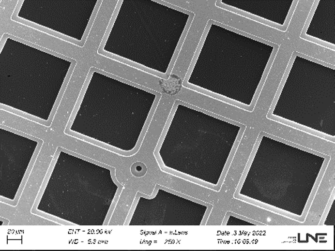
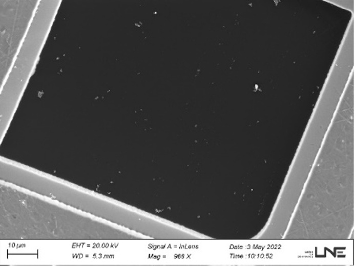
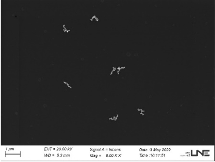
Figure 1. Nanoparticles on a TEM grid with an amorphous carbon substrate. The particles were deposited using the technique described above. Here they are seen at varying magnifications using the in-lens SE detector of the SEM.
TKD analyses were then carried out using a beam energy of 20 kV and a 120 µm aperture and high current mode, with a measurement step size of 5 nm. The results were processed using AZtecCrystal.
Results
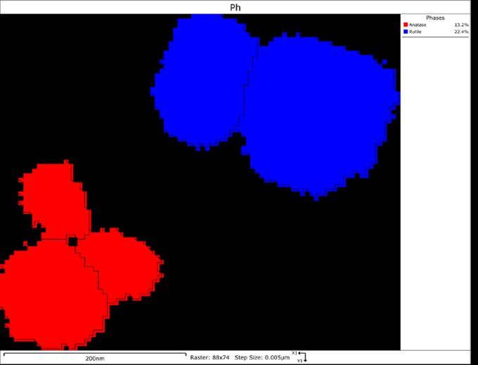
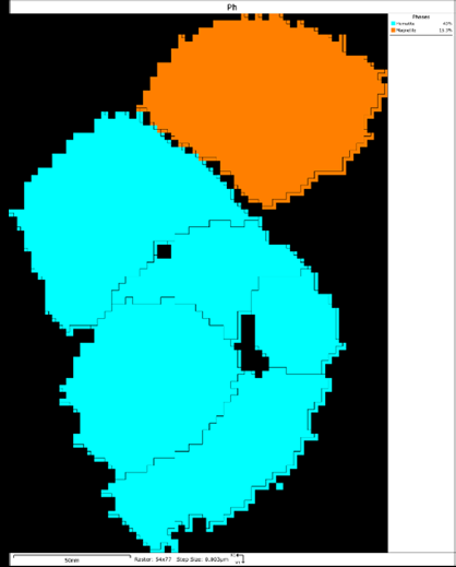
The subsequent TKD maps of TiO₂ and ferrous oxide reveal individual nanoparticles resting on an amorphous layer with no discernible crystallographic data from the carbon film (figure 2). For both nanoparticle powders, the TKD analyses have revealed indexed nanoparticles of different crystallography, chemical composition and form ranging in size from 10s to 100s nm (figure 2), highlighting the presence of both anatase and rutile in the TiO₂ powder, and hematite and magnetite in the ferrous oxide powder. This method requires no subsequent sample preparation, such as grinding, polishing, or coating, typical of EBSD analysis, and allows for the identification of individual nanoparticles as well as distinguishing between the different phases.
(a)
(b)
Figure 2. (a) Distinguishing between polymorphs of TiO₂ particles: anatase (red) and rutile (blue). (b) Separation of hematite (turquoise) and magnetite (orange) nanoparticles on a carbon film substrate.
This sample preparation method is integral for any potential analysis of nanoparticles. If these nanoparticles were prepared using traditional EBSD sample preparation techniques, the accumulation of particle aggregates would lead to the diffraction of numerous EBSPs from different types of nanoparticles or multiple nanoparticles, making the identification of EBSPs from one particle impossible.
Conclusion
This simple sample preparation technique allows for the effective analysis of nanoparticles. Here we have demonstrated the measurement of individual nanoparticles in TiO₂ and ferrous oxide powders, with robust discrimination of phases via the TKD approach using AZtecHKL and the Symmetry S2 EBSD detector. Despite the traditional notion that EBSD samples need a high degree of polish for effective analysis, this study demonstrates an alternative method. The separation and identification of nanoparticles using this technique will be discussed in a future application note.
References
- Crouzier, L., Feltin, N., Dellvallée, A., Pellegrino, F., Maurino, V., Cios, G., Tokarski, T., Salzmann, C., Deumer, J., Gollwitzer, C., Hodoroaba, V-D. (2021). Nanomaterials. 11, 3359.
- Schwarzer, R. A., Field, D. P., Adams, B. L., Kumar, M. & Schwartz, A. J. (2009). Electron Backscatter Diffraction in Materials Science, Vol. edited by A.J. Schwartz, M. Kumar, B.L. Adams & D.P. Field, pp. 1–20. Boston, MA: Springer US.

