The Applicability of Atomic Force Microscopy (AFM) in the Semiconductor Industry
Introduction
Semiconductors are an essential component in many electronic devices employed in critical industries including computing, healthcare, transportation and many others. With such a wide reach, the semiconductor industry is continuously growing and innovating with the goal of producing more energy efficient, more reliable, and more affordable devices. In order to accomplish these goals, considerable effort is directed toward the R&D and QA/QC phases of the semiconductor production cycle. Atomic Force Microscopy (AFM) is an important tool for semiconductor characterization in that cycle. Specifically, surface roughness measurements, defect review and failure analysis are areas where AFM excels and provides valuable information for semiconductor production process optimization.
Measurements of surface roughness and morphology are essential, whether to validate an individual processing step or to obtain a quality control metric for the final product. The choice of instrument best suited for surface roughness measurements depends strongly on the specific material being measured as well as on the expected size and shape of its surface features. As device dimensions in many industries continue to shrink, it is becoming increasingly important to characterize surface roughness at the scale of nanometers and even lower. Tools commonly used for this purpose include interferometric optical profilometers, scanning electron microscopes, and atomic force microscopes (AFMs) (see Table 1). AFM is the only technique offering unparalleled three-dimensional spatial resolution and the ability to measure most types of materials. AFM provides complete 3D surface quantification by imaging topography (height), as shown in Figure 1.
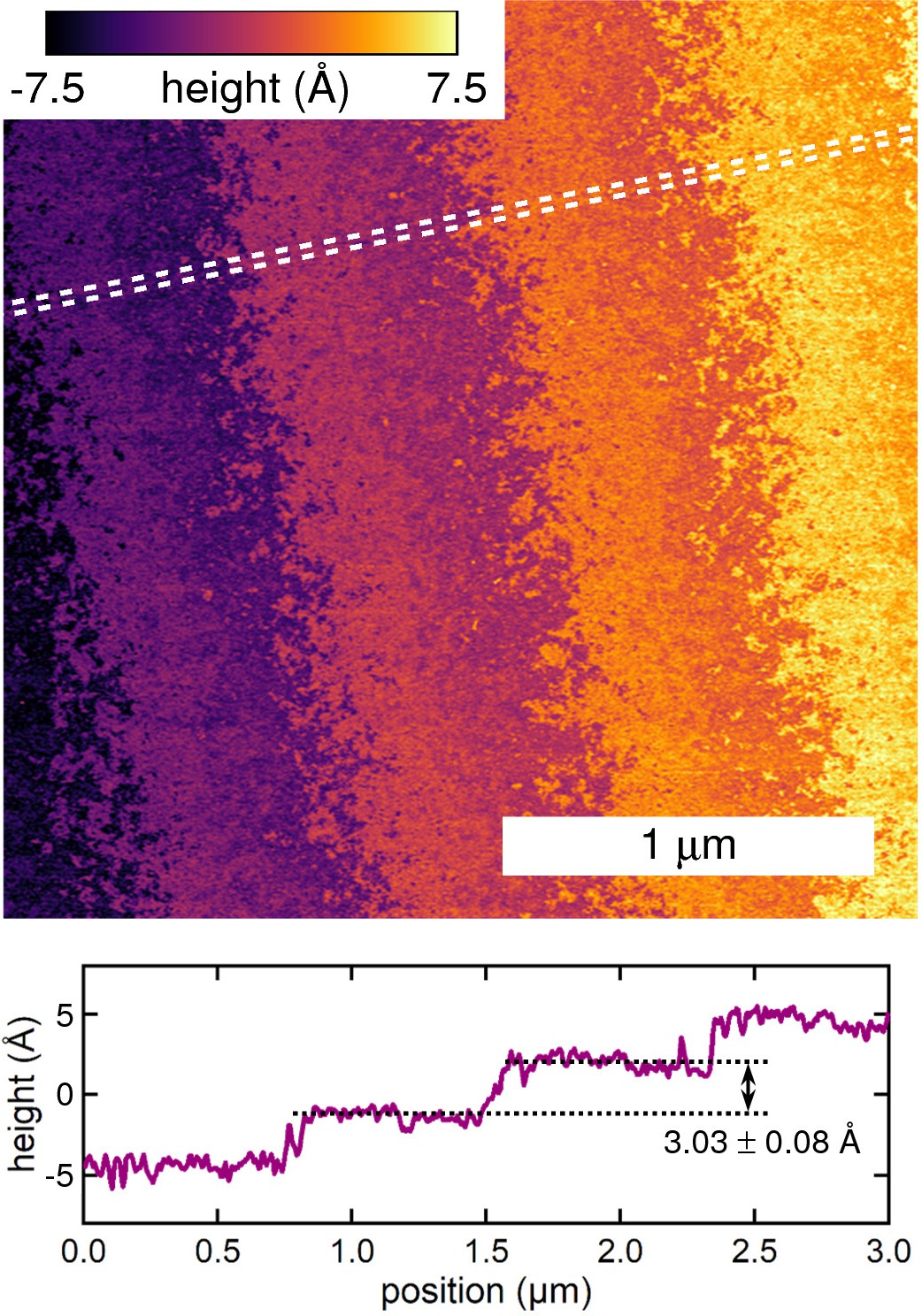
Figure 1:
Topography image of a silicon carbide wafer [6H SiC (0001)]. The graph shows the average profile between the white lines in the image and gives a step height of 3.03 ± 0.08 Å between adjacent terraces.
| Oxford Instruments Jupiter DS AFM | Scanning Electron Microscopes | Interferometric Optical Profilometers | Stylus Profilometers | Relevance |
| Lateral resolution | <1-20 nm | <1-20 nm | 200-500 nm | 1000-10,000 nm | Accurate nanoscale surface roughness measurements require nanometer-scale resolution. |
| Height resolution | <0.025 nm | No true 3D measurements possible | 1-10 nm | 0.5 nm | Accurate nanoscale surface roughness measurements require nanometer-scale resolution. |
| Measurement type | Surface topography (3D) and surface properties* | Surface morphology (quasi-3D) and composition* | Surface topography | Line profiles (inefficient for surface mapping) | Areal surface roughness measurements require accurate imaging of 3D topography. |
| Measurement time (per site) | <1 minute | <10 seconds | <10 seconds | <1 minute | Throughput of multisite measurements is affected by time spent per site. |
| Surface material limitations | Any material type can be measured up 200 mm in diameter and 35 mm in height | Must be conductive (or coated) and vacuum compatible | Large variations in reflectivity and refractive index, steep slopes or edges, and very thin films can be problematic. | Most materials can be measured unless very soft and/or sticky | Many inspection tools have constraints on the types of materials that can be measured. |
Table 1:
Comparison of tools for surface characterization. Specifications given for non-AFM tools are typical ranges for commercial instruments. Additional detailed comparisons can be found in Ref. 1. *Both AFMs and scanning electron microscopes can provide information about materials properties beyond topography. For example, AFMs can measure a host of electrical (e.g., conductivity, permittivity), mechanical (e.g., elastic modulus), and functional properties (e.g., piezoelectric response). For more information, see Ref. 2.
The Jupiter™ DS large-sample AFM: high speed AFM with top performance for surface roughness measurements
Oxford Instruments has recently introduced the Asylum Research Jupiter DS AFM (Figure 2). Jupiter leverages Asylum’s experience in developing high-performance AFMs to provide an all-new AFM with a large inspectable area, that delivers high resolution images, with reliable sub-nanometer roughness measurements coupled with high throughput and high measurement confidence. These advantages are discussed in more detail and illustrated by the case studies presented in Figures 3-5.
Jupiter DS AFM offers an 8 inch, fully addressable inspectable sample stage in its standard configuration.
Jupiter can accommodate large samples up to 210 mm in diameter and 35 mm in thickness. Alternatively, multiple smaller samples (e.g., those mounted on ~10 mm sample disks) can be magnetically mounted on the sample stage for successive inspection. The fully-addressable motorized sample stage allows images to be acquired anywhere in a 200x200 mm2 range without the need for sample rotation. The full wafer accessibility allows for quicker wafer inspection resulting in higher throughput and productivity.
Case study #1: Deposition process quality assurance
Atomic Layer Deposition (ALD) is a standard method of creating desired surface chemistry by growing materials in a controlled manner. In addition to surface chemistry, film thickness and morphology also play a critical role in the performance of a device. In this example, silicon oxide (SiO2) was grown through the ALD process (ref 3). Both, SiO2 film thickness and surface roughness were measured on several samples and the results are presented in figure 3. The data has shown that as the thickness of SiO2 increased so did the roughness, however, surface roughness increase was not increasing linearly with the oxide thickness. Specifically, surface roughness increased rapidly within the first 50 nm oxide thickness, and then slowed down and increased gradually until ~250 nm oxide thickness. There often is a target surface roughness that needs to be respected for the best device performance, in this case 100-150 pm, and determining the exact oxide thickness at which that is attained can help optimize the fabrication process which will in turn result in performant and reliable devices. This type of surface roughness analysis is only possible using AFM data as no other characterization tool can measure true 3D roughness values in the picometer range.
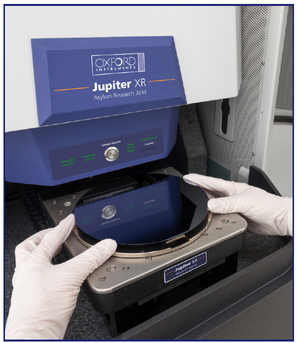
Figure 2:
The Asylum Research Jupiter DS AFM holds samples as large as 210 mm, such as this 8-in wafer.
Jupiter DS AFM: The optimal tool for nanometer-scale surface roughness measurement.
The Jupiter DS AFM easily characterizes nanometer-and angstrom-scale surface roughness on almost any material. Compared to typical large-sample AFMs, Jupiter provides higher resolution, faster imaging, and greater reliability. Compared to optical profilometry, AFMs can simply measure far smaller roughness values and a much wider range of material types and geometries. Together with its improved throughput and high measurement confidence, Jupiter DS is the ideal tool for nanoscale surface roughness measurement.
Jupiter DS ultra-low noise floor delivers unmatched sub-nm surface roughness measurements.
Asylum has applied its core of advanced AFM technology to ensure that Jupiter can measure surface roughness lower than the detection threshold of other characterization techniques. Moreover, Asylum Research AFMs can measure roughness 2-4× lower than most other AFMs. The ultra-low noise floor—the minimum resolvable height determined by mechanical and electronic instrument noise—of 0.25 Å allows the Jupiter AFM to accurately measure angstrom-scale surface roughness. Case study #2 gives an example where variations in processing conditions can be monitored though subtle changes in the surface features.
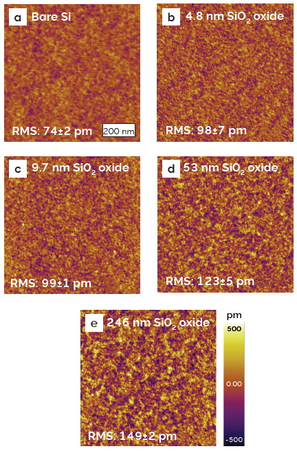
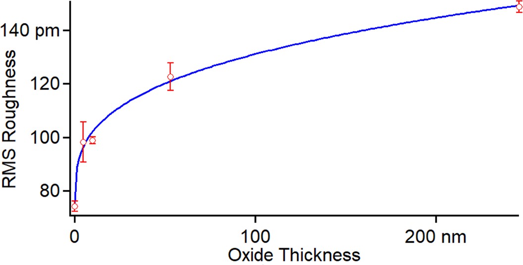
Figure 3:
Surface roughness of the SiO2 surface

Case study #2: Automated inspection of epitaxial silicon wafer roughness
Epitaxial layers are commonplace in modern semiconductor processing. Silicon epitaxy processes allow precise layers with different dopant types and concentrations, while heteroepitaxial layers of III-V compounds and other materials enable even more options. An additional benefit of epitaxial layers is their extremely low surface roughness compared to substrates prepared by chemical-mechanical polishing. Figure 4 shows an example of roughness measurements on a wafer with an epitaxial silicon layer. It demonstrates Jupiter’s ability to make angstrom-level roughness measurements as well as automating measurements at different sites on the wafer.
Exclusive blueDrive™ cantilever excitation enables high measurement confidence and reliability. Surface roughness measurements often influence critical business decisions, so it is vital that measurements are trustworthy and the instrument is reliable. Asylum’s exclusive blueDrive tapping mode technology improves imaging stability compared to conventional AFMs that use piezo excitation. This extends tip lifetime and in turn makes roughness results more consistent and repeatable (see Case study #3, Figure 5).
Jupiter DS AFM allows for high throughput and increased productivity. Jupiter can image 5-20x faster than most AFMs, such that single images can routinely be acquired in less than 2 minutes and as little as 15 seconds (depending on scan range and overall roughness). In addition, its high-speed motorized sample stage moves between sites in 5 seconds or less with micrometer precision. High-speed scanning and positioning are especially valuable when combined with Jupiter’s capabilities for automatic image acquisition as described in case study #3 (see Figure 5).
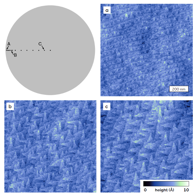
Figure 4:
Non-uniform grain size is often observed in epitaxial silicon layers, especially near the wafer edge where greater variations in process conditions may occur. As shown in the diagram, a series of locations on a 150-mm (6-in) wafer were pre-defined in software and used in an automated routine to acquire topography images. a) Image acquired 200 μm from the wafer edge with Sa=0.785 Å. b) Image at 1.6 mm from the edge with Sa=0.833 Å. c) Image acquired 62.4 mm from the edge (12.8 mm from the center) with Sa=0.902 Å.
Case study #3: Quality control of disk drive media
Magnetic hard disk drives continue to dominate over solid state drives in applications that require massive amounts of inexpensive data storage. This advantage has been maintained by continued increase in the data storage density of magnetic disk media. Achieving these high densities has required a corresponding decrease in media roughness. The example in Figure 5 shows roughness measurements on the substrate of a modern lubricated disk media. With 1000 images acquired unattended over 15 hours, it demonstrates Jupiter’s extreme measurement fidelity as well as its high measurement throughout.
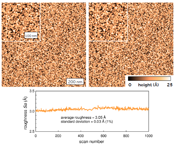
Figure 5:
These topography images of a glass disk media substrate are the first and last in a sequence of 1000 acquired over 15 h of unattended operation (~54 seconds per image). In each image, the inset is a digitally zoomed magnification of the lower left region to help show the finer structure. The graph shows that the measured roughness
Sa remains constant within 1% over the entire period, demonstrating the remarkable stability enabled by blueDrive tapping mode imaging.
Case study #4: Defect review to prevent future failures
Defects on substrates used for thin films deposition often affect the resultant thin film morphology that can result in subsequent failures in finished devices. In the examples below, AFM was used to characterize the surfaces of thin films in order to better understand and prevent device failures.
Indium arsenide (InAs) is semiconductor which is used in infrared detectors. Topography image of InAs grown on gallium antimonide (GaSb) substrate is shown in figure 6a. The surface exhibits regular steps with the exception of a large “island” that is much higher than the rest of the surface features. It is possible that, a defect originally present on the GaSb substrate favored InAs film growth which resulted in this unwanted high profile island at this specific location. Presence of such a defect on the InAs film may correlate with decreased performance of the detector so further treatment of the GaSb substrates prior to InAs deposition will be investigated. The other example of defect review is gallium nitride (GaN) thin films grown on sapphire which are used in high frequency and high voltage applications. Topography image in figure 6b, shows unexpected hexagonal defects (holes) in the GaN thin film. Additional analysis of the sample using various electrical AFM modes such as scanning capacitance microscopy (SCM), conductive AFM and Kelvin probe force microscopy (KPFM), indicated that the defects have an electrical signature that may cause failure during high voltage applications.
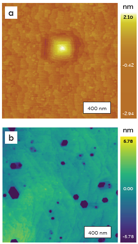
Figure 6: a) InAs film grown on GaSb, b) GaN film grown on sapphire
Jupiter DS AFM: The optimal tool for nanometer-scale surface roughness measurement
The Jupiter DS AFM easily characterizes nanometer and angstrom-scale surface roughness on almost any material. Compared to typical large-sample AFMs, Jupiter provides higher resolution, faster imaging, and greater reliability. Compared to optical profilometry, AFMs can simply measure far smaller roughness values and a much wider range of material types and geometries. Together with its improved throughput and high measurement confidence, Jupiter DS is the ideal tool for nanoscale surface roughness measurement.
References
- P. J. D. Whiteside, J. A. Chininis, and H. K. Hunt, Coatings
- 6 , 35 (2016).
- For more resources on AFM characterization of thin films, see https://afm.oxinst.com/thin-films
- Iacona, Fabio, et al. "Roughness of thermal oxide layers grown on ion implanted silicon wafers." Journal of Vacuum Science & Technology B: Microelectronics and Nanometer Structures Processing, Measurement, and Phenomena 16.2 (1998): 619-627.

