Surface Engineering for High Performance Qubits
Oxford Instruments is at the heart of the quantum computing revolution. From creating the cryogenic environments where devices operate to the precision manufacture of those devices, we understand and solve the challenges. Oxford Instruments Plasma Technology has nearly 40 years of experience collaborating with leading researchers on process solutions for a wide range of materials and device structures, and our process library of over 7,000 recipes spans the elements and material compounds. We work closely with the quantum community and we know how to minimize losses arising from device processing. In this white paper we will review how surfaces and interfaces have a strong effect on losses and how plasma processing can be used to control those losses.
Many of quantum computing's leading researchers and companies have studied the impact of surface engineering on superconducting resonator and qubit performance, including Will Oliver, David Pappas, John Martinis, and Rigetti Computing. The body of literature in this area shows that the performance of even the simplest element of quantum computers, the superconducting LC resonator, is dramatically impacted by subtle details of device fabrication. Surfaces are known to be critical to the fabrication of high-performance quantum devices of all kinds, including color centers, ion traps (which can suffer from surface electric field noise), photonics, and quantum dots. This whitepaper will focus on superconducting quantum devices, but many of the principles and strategies used to optimize interfaces for these systems are also relevant for devices of all kinds, both quantum and classical.
There are three critical surfaces, or interfaces, that must be controlled in order to make high quality superconducting resonators and qubits. These are (1) the superconducting metal-substrate interface (MS), (2) the superconducting metal-air interface (MA), and (3) the substrate-air interface (SA). Qubits are extremely sensitive to any sources of loss in these interfaces. Sources of loss may include unwanted oxides, surface adsorbates like hydroxides, resist residuals, crystal defects, surface roughness, and other contaminants. Great efforts have been made to minimize the proportion of the electric fields in the qubits traveling through these lossy interfaces — engineering the participation ratio as in 3D cavity resonators or with the use of superconducting caps, which can be fabricated with Oxford Instruments Plasma Technology's PlasmaPro®100 Cobra and PlasmaPro®100 Estrelas etch systems — but ultimately some level of interaction is unavoidable in practical systems. High quality tools, targeted process solutions, and a deep understanding of how those processes affect the surfaces and interfaces are necessary to minimize loss.
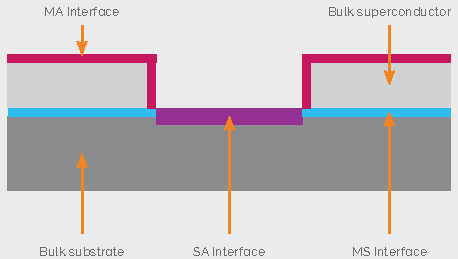
Fig. 1 — Key Interfaces in Superconducting LC Resonators. (1) Metal-Air: MA, (2) Metal-Substrate: MS, (3) Substrate-Air: SA.
Key Metrics
The most common reported metric in superconducting resonator studies is the internal quality factor, Qi. Qi is a measure of the extent to which a resonator's actual performance matches up with its designed performance, which can be predicted very accurately for simple designs. The inverse of Qi, 1/Qi, is equal to the loss tangent. The loss tangent is usually denoted as tan δ, or occasionally just as δ (since tan δ ≈ δ for small δ). Losses are additive, such that the overall 1/Qi can be decomposed into a series of constituent losses from each contributing mechanism, such as loss due to bulk silicon, surface roughness, superconductor surface oxide, or a host of other contributing factors, where in general 1/Qi = psource_1/qsource_1 + psource_2/qsource_2 +…, where psource_n is the participation ratio of the electric field in a given loss source and qsource_n is the quality factor due to a given loss source. It is ideal for the internal quality factor to be reported at single photon excitation energies, which in turn requires cryogenic temperatures on the order of 10–100 mK. Broadly, as of this writing, a "good" internal quality factor is somewhere in the range of 1–2M for a conventional 2D geometry, while anything under 100k is considered poor and anything above 2M is superb depending on specifics.
Qubit coherence time T1 is roughly related to Qi by the relation T1 = Qi/(2πf01), where f01 is the qubit operational frequency (typically 4–8 GHz). Though the increased complexity of qubit fabrication and design complicates direct comparison of resonator Qi to qubit T1, this relation can be helpful as a very approximate metric in the right context. Qi of 1M roughly corresponds to a T1 of 20–40 μsec using the relation described above, which has been consistently achieved in the field, while Qi of 5M roughly corresponds to 100–200 μsec, which is indeed at the upper limit for current silicon-based transmon qubits.
Achievable quality factors are limited primarily by surface losses. Sapphire has very low bulk loss and could theoretically achieve Q on the order of 109 according to one recent study. The loss tangent of bulk silicon limits 2D resonator internal quality factor to a maximum of approximately 5.5M, assuming a bulk participation ratio pbulk of 90% and qbulk of 5M. By comparison, the superconductor bulk itself limits internal quality factor to 10M (assuming psuper = 1% and qsuper = 100k). The limiting factor for internal quality factor is surface losses, even in cases where the electric field's participation in these layers is under 0.1%. In practice, these participation ratios can vary widely based on specific design and the specific material quality factors are imprecise.
Unsurprisingly, measured values for internal quality factor vary depending on resonator design and measurement setup even for similar material systems, adding difficulty to direct comparison. The absolute value of Qi achieved in any given study is ultimately less instructive than the clarity with which the study is able to identify and distinguish loss factors so that they might be optimized in the future.
Superconducting Metal-Substrate Interface
The superconducting metal-substrate interface (MS) is defined by (1) the condition of the substrate prior to pre-treatment, (2) the pre-treatment itself, (3) any oxidation or aging effects prior to superconductor deposition, and (4) any damage or strain at the interface induced by the superconductor deposition process. Most of the published work on resonators has been carried out on high resistivity silicon and sapphire due to their relatively low bulk loss tangents. It is common to pre-treat silicon substrates with HF shortly before superconductor deposition in order to remove native oxide without roughening. The DiCarlo group used HF treatment to remove Si surface oxide and followed it with treatment with HMDS, which is a hydrophobic material used in many photolithography processes. They used XPS to study the effect of HMDS in slowing the reoxidation of the Si surface. They also measured resonators prepared with and without HMDS pretreatment and found that there was a relatively consistent improvement in the performance of resonators fabricated with the HMDS pre-treatment. This work was successfully verified and expanded on by Rigetti Computing. In situ plasma pretreatments to remove amorphous native oxide and control substrate surface termination are possible but have not been studied for quantum technology applications.

Fig. 2 — (a) 200 nm Nb etched to SiO₂, (b) 300 nm Nb film etched down to SiO₂ with slope achieved by PR erosion and low selectivity process, (c) Nb etch with vertical profile, (d) Etched Al features and clean PR strip without any post-etch corrosion.
Superconducting Metal-Air Interface
The next important interface is the superconducting metal-air interface (MA). The key factors in this interface are oxidation of the superconductor surface and the quality of the superconductor itself, in terms of crystallinity and defect density. The most common superconducting resonator material, Nb, offers easy deposition and etch along with a high Tc convenient for 4K testing, at the cost of significant mixed surface oxide thickness. Oxide composition and thickness are major concerns in superconducting qubit devices because they are significant sources of loss and thus degrade both resonator internal quality factors and qubit coherence times. The Siddiqi group at the University of California, Berkeley recently announced that they achieved exceptionally high Qi of 5M on a Nb/Si superconducting resonator system by etching the native Nb oxide in 5:1 Buffered Oxide Etch for 20 minutes (long enough to remove approximately 10 nm of Nb2O5) immediately prior to packaging and cooldown. Although perhaps incompatible with most fully integrated device architectures, this result demonstrates quite clearly that surface oxide minimization is crucial to minimize losses in superconducting devices. Similarly, a recent paper by Princeton University found that HIPIMS (High-Power Impulse Magnetron Sputtering) deposition, typically used to encourage dense film formation, led to smaller grain sizes and increased undesirable Nb surface oxide, which together led to decreased coherence time in their qubit fabrication process. The researchers hypothesized that other materials, such as Tantalum, may outperform Nb due to their more homogenous surface oxides. The researchers then went on to study the tantalum system. They found that BCC α-phase Ta on sapphire outperformed Nb-based qubits by a wide margin, achieving coherence times on the order of 200–300 μs. Tantalum's surface oxide is thinner (2–3 nm) and less lossy than Nb surface oxide (8–10 nm) after processing. Superconducting sputtered Tantalum must be deposited at or above 500°C to achieve the preferred BCC α-phase, however, and it is unknown whether similar performance is possible on a silicon substrate. Princeton's team etched Ta with a wet process because their in-house RIE process was unable to achieve smooth edges. Oxford Instruments Plasma Technology offers a smooth Ta etch process with our ICP RIE tools which was successfully used for this application by scientists at Alibaba to achieve superconducting resonators with Qi in excess of 1.5M in similar experiments with Ta on Sapphire.
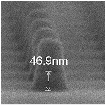
Fig. 3 — 60 nm Ta features etched down to SiO₂ with Oxford Instruments etch tool.
Superconducting nitrides may offer improved performance over elemental metal superconductors. NbTiN, for example, has a stable and thin 1.5 nm oxide and was used to achieve internal quality factors in excess of 1M for superconducting resonators as early as 2015. Since that time, Will Oliver's research group at MIT Lincoln Labs determined that TiN is less lossy than Al and researchers at Alibaba recently disclosed that they achieve Qi as high as 3M with epitaxial TiN on sapphire. The Siddiqi group has also achieved very high internal quality factors by capping pre-etched Nb resonators with a layer of TiN.
Superconducting nitrides are also desirable for applications which take advantage of kinetic inductance in films on the order of 5–10 nm thickness. Kinetic inductance can be a useful parameter for some designs, as well as for other quantum technology applications, including hybrid circuit elements, SNSPDs, and superinductors. Oxford Instruments Plasma Technology's FlexAL ALD system can be used to deposit extremely uniform thin films and our market-leading bias control can be used to tune film crystallinity and other parameters to optimize the performance of these types of devices.
ALD nitride superconductor depositions offer many advantages as compared to PVD, including superior reproducibility, composition, and thickness control. This is both because precursor chemicals are not reused run-to-run in the sense that a sputter target is eroded over time and poisoned during nitride/oxide processes, and also because both thickness and composition are easily controlled by the number, timing, and sequence of ALD cycles, even for complex materials. ALD is commonly used for critical depositions in mature high-performance applications for these reasons. ALD techniques will also play a critical role in the future maturation of 3D superconducting interconnects because of the superior conformality of ALD, which is a non-negotiable requirement for many 3D superconducting structures, such as superconducting through silicon vias. It is likely that superconducting quantum device fabrication will follow a trend similar to that observed in the commercial semiconductor industry, where ALD has become increasingly critical for high performance devices over time.
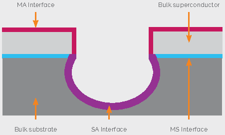
Fig. 4 — "Trenched" superconducting resonator. Bulk substrate material is removed to reduce the participation ratio of electric fields in the lossy SA Interface as well as within the bulk substrate itself. The creation of excess SA Interface surface area is acceptable because the added surface is further from the high-field region near the gap between superconductors.
Substrate-Air Interface
The substrate-air interface (SA) has been studied by many of superconducting quantum computing's leading researchers, including both Will Oliver's group and the DiCarlo group. In the simplest conception, the goal is to remove excess substrate and minimize the proportion of the electric field that travels through both the substrate itself and this interface. This has been attempted in rather dramatic fashion by using isotropic and anisotropic dry etches to remove substrate material between and/or underneath the superconducting metal. This technique is sometimes referred to as "trenching" based on the visual appearance of completed samples. In practice, however, trenching alone is not always sufficient to achieve optimal performance.
Silicon (and sapphire, which is sometimes used as an alternative), though a potential loss source that can be removed, has a much lower loss tangent in its bulk than the contaminants, oxides, defects, and other imperfections that are present on a real surface after processing. Simply removing the maximum amount of material, then, is not a guaranteed path to optimal performance. Factors that can affect loss in this interface include the etch depth, sidewall angle, roughness, degree of undercut of the superconductor material, the chemical termination of the substrate, and the presence of residues and other contaminants at the substrate-vacuum interface. In some cases, less aggressive etches have outperformed etches that removed more material. Work by Dave Pappas' group at NIST in 2012 showed that, for a similar trenched etch profile, a F-based Silicon termination had less than half the loss of a Cl-based termination. Cl etches are known to leave difficult-to-remove salts and can in some cases even corrode superconducting metals.
Some processes can also induce surface roughness, especially extreme trenching processes. One example of this was work by the DiCarlo group, where they used Deep Reactive Ion Etching (DRIE) to remove as much substrate as possible between the resonator lines. They achieved internal quality factors in excess of 1M with a DRIE Bosch etch process and NbTiN resonators but observed sidewall roughness on the order of 100 nm and also pointed out the potential for additional losses due to the passivation layer resulting from Bosch etch processes. Poor superconductor etches can also be problematic. As many superconductors are etched with chemistries that also etch silicon, it is possible for superconducting material to be unintentionally undercut or for silicon to be roughened by the chosen etch chemistry, increasing loss at the SA interface. A highly selective etch with a good post-clean process and low induced surface damage may enable development of lower-loss resonators and provide related insight into better approaches to improving qubits themselves. Oxford Instruments offers excellent plasma tools and deep process expertise for etching both substrate and superconducting metal materials. Our PlasmaPro®100 Estrelas Deep Silicon Etching etch solution can achieve passivation-free and smooth, scallop-free sidewalls with excellent sidewall angle control, which both reduces loss at the SA interface and enables sophisticated profile engineering to ensure that conformal superconducting metal can be easily deposited on sidewalls with both ALD and PVD techniques to ensure high TSV yield. Oxford Instruments Plasma Technology also has significant experience etching sapphire for a wide variety of applications. In addition, for superconducting metal etch, we offer tools with an enormous range of well-defined processes for isotropic and anisotropic etches of a wide variety of superconducting materials such as Al, Nb, Ta, TiN, and NbN. For quantum color centre applications, our Cobra 300 diamond etch tool offers unique market-leading low-roughness performance for diamond etches with O termination, and we also have significant experience etching emerging color center materials such as SiC and TiO2. We also have extensive experience with both etch and deposition of 2D materials such as graphene and hBN, which are increasingly of interest for a wide variety of quantum device applications, including Josephson Junction barriers, single photon emitters, and state-preserving hybrid transducers.
Conclusions
The field of superconducting qubits is still far from maturity. A wide range of challenges remain to go beyond NISQ, from the practical puzzle of scalable 3D integration to the subtle difficulties of quasiparticle trapping and qubit design. In this whitepaper, we have focused on a small subset of work on perhaps the most basic element of superconducting quantum computers — the resonator. If you are working on quantum devices, we would love to talk and learn about your device fabrication challenges and how we can help, both in the long-term — through collaborations and partnerships — and in the short-term — by providing you with the plasma tools you need to achieve your goals. We hope this article helps in your quantum device fabrication journey and we look forward to speaking with you soon.
References
- Calusine, Greg, et al. "Analysis and mitigation of interface losses in trenched superconducting coplanar waveguide resonators." Applied Physics Letters 112.6 (2018): 062601.
- McRae, Corey Rae Harrington, et al. "Materials loss measurements using superconducting microwave resonators." Review of Scientific Instruments 91.9 (2020): 091101.
- Wenner, J., et al. "Surface loss simulations of superconducting coplanar waveguide resonators." Applied Physics Letters 99.11 (2011): 113513.
- Nersisyan, Ani, et al. "Manufacturing low dissipation superconducting quantum processors." 2019 IEEE International Electron Devices Meeting (IEDM). IEEE, 2019.
- Kaviani, Moloud, et al. "Proper surface termination for luminescent near-surface NV centers in diamond." Nano letters 14.8 (2014): 4772–4777.
- Brown, Kenneth R., et al. "Materials Challenges for Trapped-Ion Quantum Computers." arXiv preprint arXiv:2009.00568 (2020).
- Eriksson, M. A., S. N. Coppersmith, and M. G. Lagally. "Semiconductor quantum dot qubits." MRS bulletin 38.10 (2013): 794–801.
- Wang, Chen, et al. "Surface participation and dielectric loss in superconducting qubits." Applied Physics Letters 107.16 (2015): 162601.
- O'Brien, William, et al. "Superconducting caps for quantum integrated circuits." arXiv preprint arXiv:1708.02219 (2017).
- Houck, Andrew. "New material platform for superconducting transmon qubits with coherence times exceeding 0.3 milliseconds" [Conference Presentation]. APS March Meeting 2021.
- Lei, Chan U., et al. "Multilayer Microwave Integrated Quantum Circuits" [Conference Presentation]. APS March Meeting 2021.
- Melville, Alexander, et al. "Dielectric Loss in Titanium Nitride and Aluminum Superconducting Resonators" [Conference Presentation]. APS March Meeting 2021.
- Bruno, A., et al. "Reducing intrinsic loss in superconducting resonators by surface treatment and deep etching of silicon substrates." Applied Physics Letters 106.18 (2015): 182601.
- Ahles, Christopher, et al. "A Dry NF3/NH3 Plasma Clean for Removing Si Native Oxide and Leaving a Smooth Si Surface". 2018 MRS Spring Meeting & Exhibit, April 2–6, 2018, Phoenix Arizona.
- Premkumar, Anjali, et al. "Microscopic Relaxation Channels in Materials for Superconducting Qubits." arXiv preprint arXiv:2004.02908 (2020).
- Banerjee, Archan, et al. "Process Optimization for Superconducting Resonators via Identification and Mitigation of Interface Loss Mechanisms" [Conference Presentation]. APS March Meeting 2021.
- Place, Alex PM, et al. "New material platform for superconducting transmon qubits with coherence times exceeding 0.3 milliseconds." arXiv preprint arXiv:2003.00024 (2020).
- Zhang, Xiaohang, et al. "A study of intrinsic dielectric loss of tantalum based superconducting quantum circuits" [Conference Presentation]. APS March Meeting 2021.
- Zichi, Julien. NbTiN for improved superconducting detectors. Diss. KTH Royal Institute of Technology, 2019.
- Melville, Alexander, et al. "Comparison of dielectric loss in titanium nitride and aluminum superconducting resonators." Applied Physics Letters 117.12 (2020): 124004.
- Morozov, Dmitry, et al. "Design and characterisation of titanium nitride subarrays of kinetic inductance detectors for passive terahertz imaging." Journal of low temperature physics 193.3 (2018): 196–202.
- Burkard, Guido, et al. "Superconductor-semiconductor hybrid-circuit quantum electrodynamics." Nature Reviews Physics 2.3 (2020): 129–140.
- Knoops, Harm CM, et al. "Status and prospects of plasma-assisted atomic layer deposition." Journal of Vacuum Science & Technology A: Vacuum, Surfaces, and Films 37.3 (2019): 030902.
- Sandberg, Martin, et al. "Etch induced microwave losses in titanium nitride superconducting resonators." Applied Physics Letters 100.26 (2012): 262605.
- Tolpygo, Sergey K., et al. "Advanced fabrication processes for superconductor electronics: Current status and new developments." IEEE Transactions on Applied Superconductivity 29.5 (2019): 1–13.

