Aim: To measure the quality of transistor components in the most efficient and cost effective way possible
Challenge
Semiconductor devices are fabricated using a variety of materials, making it crucial to be able to understand and quantify what elements are present and to correlate elemental distribution with specific micron size device regions. As semiconductor devices continue to downsize, there is a need for high spatial resolution analysis – which is often performed with the TEM – in a process which is often time-consuming and complex.
Solution
Instead of performing TEM analysis, an electron transparent sample containing a region of interest is loaded into a TKD sample holder in a SEM. An Ultim® Max 170 large area silicon drift detector is then used together with a high accelerating voltage to perform a transmission analysis of the sample's composition at high spatial resolution.
Results
Figure 1 shows the distribution of the elements in the device. These maps were collected in just 5 minutes and contain a total of 16 million x-ray counts. The distribution of N corresponds well to Ga (GaN) and Si (SiNX) distribution, Ti and Ni 100 nm size regions are clearly visible. The advanced TruMap® function in AZtecLive has successfully resolved peak overlaps involving the N-K and Ti-L lines to ensure that true spatial distributions are shown.
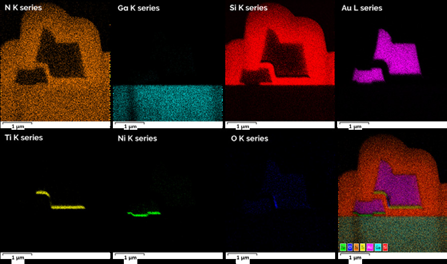
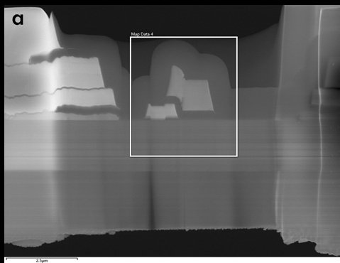
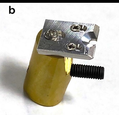
Figure 1: The TruMap elemental distributions of N, Ga, Si, Au, Ti, Ni, O collected with STEM-EDS Ultim Max 170 at 30 kV. a) STEM image of the sample. b) Sample holder.
Conclusion
Ultim® Max 170 used in a STEM-EDS setup provides a realistic and effective alternative to TEM based analysis for the high spatial resolution (<100 nm) requirements of elemental mapping that are necessary for the fast and cost effective characterisation of high frequency and power GaN devices.

