Photon counting is a technique used to detect individual photons and minimise noise in a range of imaging and spectroscopy experiments that study extremely faint light sources:
- Reading the register of an ion-trap quantum computer by detecting the weak fluorescence of confined and entangled ions [e.g. 1,2].
- Studying the quantum properties of entangled photons for fundamental physics research, development of quantum imaging techniques, and application to both quantum information processing and communications [e.g. 3-8].
- Developing and testing materials for use as precision quantum light sources in optical computing and communications [e.g. 9].
This article discusses how photon counting is achieved with different sensor technologies, namely Electron-Multiplied Charge Coupled Device (EMCCD) sensors and Complimentary Metal-Oxide-Semiconductor (CMOS) sensors. Achieving single-photon sensitivity/resolution is an exercise in noise mitigation, so the sources of spurious noise that ultimately limit each technology's photon resolving capability will also be addressed. For EMCCD sensors this noise is Clock Induced Charge (CIC); for CMOS sensors it is Random Telegraph Noise (RTN).
Photon Counting with EMCCD Cameras
In EMCCD sensors photons that interact with the photosensitive region of the sensor's pixels generate photoelectrons. At readout these photoelectrons are clocked vertically into the sensor's shift register before the shift register clocks them horizontally pixel-by-pixel into the sensor's readout amplifier. All pixels are read through the same amplifier and therefore have read noise drawn from the same read noise distribution.
The typical read noise imparted to a signal by an EMCCD's readout amplifier is at least 2 or 3 e-, even in a slow scan low noise read mode. This results in a Signal-to-Noise Ratio (SNR) below unity for a single signal electron (in other words, a signal cannot be resolved to single-photon precision). To overcome this limitation an EMCCD's electron multiplying readout register can multiply the number of signal electrons through high voltage clocks that cause impact ionisation as the charges shift from one pixel to another. There is a chance that the electrons will be multiplied at each clock through the register, so it's possible to greatly multiply the number of signal electrons (by factors up to 1000) by the time they reach the readout amplifier. With this multiplication the relative Signal-to-Noise Ratio (SNR) of a single photoelectron can be boosted to levels that render the read noise effectively negligible (i.e. noise < 0.1 e-, SNR > 10). More details about how EMCCD cameras work can be found on the Andor Learning Centre.
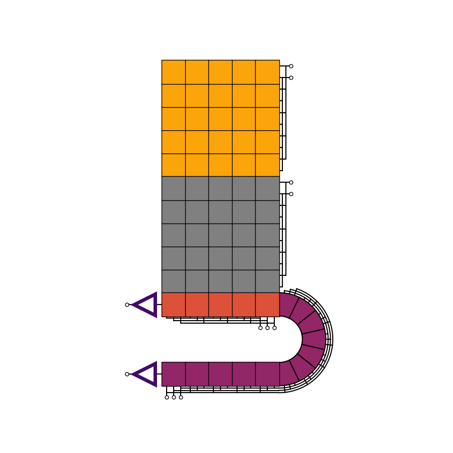
Figure 1 – Diagram representing the design of the EMCCD sensors incorporated into Oxford Instruments iXon EMCCD cameras. The optically exposed imaging area of the sensor is shown in yellow. The optically masked region shown in grey is a frame transfer area used to reduce the sensor’s imaging cycle time. The red row of pixels is a conventional readout register, allowing the camera to double as an EMCCD and a conventional slow scan CCD. The longer purple register is the EM gain register that supports signal amplification through high voltage clocking. The conventional and EM gain registers each have a separate readout amplifier. Black lines and nodes represent charge clocking circuitry.
Although the signal of a single photon can be multiplied to a detectable level, the probabilistic nature of the multiplication process results in a multiplicative noise factor that increases photon shot noise by a factor of and limits the camera's ability to resolve individual photon counts. In other words, we might be sure that the signal is there, but it's not necessarily possible to tell the difference between a detection of a single photon or two photons. Innovative techniques in camera operation and data post-processing allow us to circumvent this issue, however.
Operating the camera with high EM gain ensures each photon is detected clearly above the read noise. Running the camera at high frame rates at the same time ensures that there is only enough time for a maximum of one photon to be detected per pixel per frame. By measuring the number of counts reported by the camera under dark conditions, it becomes possible to define a threshold level of counts that must be reached to register a photon detection. When a kinetic series of images is recorded and processed in this way, the result is a set of images with binary dynamic range where each pixel records either a detection or a non-detection of a single photon. With the certainty that each detection in a frame represents only one photon, the multiplicative noise factor is effectively nullified. Deeper images with single photon intensity resolution can then be built up by adding binary frames together. Because this photon counting technique relies on having a single electron per pixel per frame at most, it works best when imaging extremely faint light sources.
EMCCD Noise Sources When Photon Counting
When imaging with photon counting mode it is critical to minimise false-positive detections. Remember that image spikes caused by hot pixels and CIC cannot be distinguished from photon detections by their intensity because all pixels with counts above the threshold are treated as a single photon detection. Because the EM gain register cannot distinguish between electrons from different sources, extra noise electrons generated by hot pixels and CIC are multiplied just the same as the signal electrons we want to amplify. CIC and hot pixel electrons therefore need to be eliminated at source.
Hot pixels are pixels on the EMCCD sensor array that are highly sensitive to temperature and have anomalously high dark current in comparison to the sensor's average. Even in short exposures hot pixels can show up as bright spikes in images if the sensor is warm. Deep sensor cooling is used to mitigate the dark current in these pixels and ensure that their value remains below the threshold unless they detect a photon. For example, the iXon ULTRA EMCCD camera relies on a multi-stage thermoelectric cooler and housing the sensor in a secure vacuum chamber to ensure that the sensor's temperature can be reliably held at values as low as -100 C.
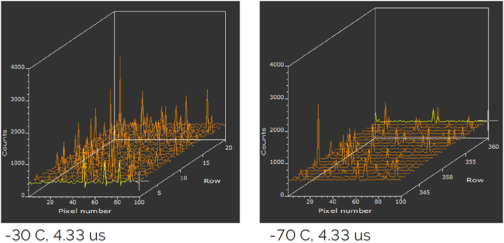
Figure 2 - 3D projection of hot pixels and Clock Induced Charge present in bias frames taken with an iXon ULTRA 888 EMCCD camera. Vertical clock speed is held constant at a relatively long 4.33 µs in both frames, but the frame on the left is taken with the sensor at a higher set temperature that results in a much greater degree of hot pixel contamination. In the frame on the right, most of the remaining spikes are the result of CIC.
CIC is the addition of electrons to pixels during pixel clocking caused by impact ionisation events within the silicon. It occurs under normal circumstances in any CCD, but without electron multiplication it is normally buried in the read noise. The process that generates CIC is like that used for electron multiplication except that it occurs where and when we don't want it. CIC can be generated during any clocking cycle, whether vertical or horizontal, but most of the CIC events detected in images appear when charges are being vertically clocked down through the sensor array toward the readout register [e.g. 10]. Because the odds of generating CIC increase with the amount of time it takes to complete a clocking cycle [10], it can be minimised by optimising precise and very rapid vertical clocks. Andor has engineered fine temporal control over the clocking in its iXon EMCCD cameras; particular focus has been placed on shaping the clock edges at nanosecond resolution to minimise the generation of CIC electrons to a rate of 0.005 per pixel per frame or lower.
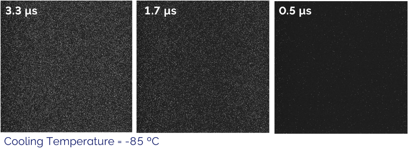
Figure 3 – Clock Induced Charge shows up at bright pixels in these unilluminated bias images from an iXon ULTRA 888 EMCCD camera. The sensor cooling temperature is constant for all frames at -85°C to mitigate hot pixels. Images taken with faster vertical shift speeds (clocking cycle times at top left of each frame) show noticeably less CIC contamination.
After dark current and hot pixel suppression, CIC is the last source of noise that has a meaningful effect in photon counting with EMCCDs. Because CIC generation is a probabilistic process it is somewhat possible to mitigate its presence in a series of images during the stacking process used to build up a deeper photon-resolved image. In a single frame, however, CIC defines the ultimate detection limit in photon counting mode.
Photon Counting with CMOS Cameras
Unlike EMCCDs, CMOS sensors have a highly parallel architecture. Rather than being clocked across the sensor to reach a single readout amplifier, each pixel converts signal charge to voltage through its own individual amplifier. This parallel architecture provides the benefit of very rapid readout for large format sensors, but this is achieved at the expense of sensor uniformity. While the ideal CMOS sensor would have similar and well behaved (i.e. Gaussian) read noise distributions for all its pixels, it is impossible to manufacture a device with the complexity of a multi-megapixel CMOS sensor without the presence of at least a few imperfections and defects. Indeed, when a long series of bias frames is obtained with a CMOS camera most pixels will have narrow Gaussian read noise distributions (often representing read noise of order 1 e- or less). The average read noise distribution of the full CMOS sensor invariably has a long tail, however, because there will always be a subset of pixels with broad and non-Gaussian read noise distributions resulting from the effects of Random Telegraph Noise (RTN).
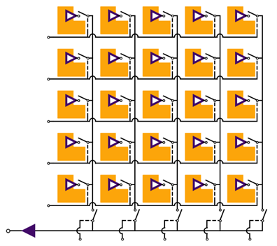
Figure 4 – Diagram representing the design of a CMOS sensor. As in Figure 1, the optically sensitive region of each pixel is shown in yellow. Note that each pixel has its own readout amplifier which converts charges to a voltage that’s then sent to an analog-to-digital converter (ADC) for digitisation. Unlike this diagram, many CMOS sensors have one ADC catering to each pixel row, or a cluster of pixel rows.
Random Telegraph Noise in CMOS Imaging
RTN is a well-documented phenomenon in MOSFETs measured as abrupt step changes in voltage or current between two or more discrete values at random points in time. It is predicted to be the result of random trapping and release of charge carriers at defect sites within a transistor's gate-oxide or at the interfaces of its component materials [e.g. 11, 12]. RTN manifests in imaging data as discrete offsets in the number of counts recorded from frame to frame that are uncorrelated with the number of photons detected.
CMOS sensors are much more susceptible to RTN than CCD sensors because of their more complex architecture and the presence of multiple transistors in each pixel. As previously mentioned, it's impossible to guarantee uniform performance for all pixels in a multi-megapixel sensor; a certain percentage of them will have defects despite the manufacturer's best efforts to eliminate them. For example, if defects affect only ~0.1% of pixels on a 4 Megapixel CMOS sensor, we can expect ~4000 pixels to be affected. Studies of RTN in CMOS sensors suggest that the proportion of pixels affected by RTN in a CMOS sensor could be as high as 10% in some cases, but the strength of the RTN (i.e. the size of the observed offsets from baseline) also varies significantly from pixel to pixel [12].
Studies of RTN in scientific CMOS cameras show that most pixels are well behaved and have read noise distributions that can be characterised by a single Gaussian function with a full width at half-maximum close to the median read noise value of the sensor [e.g. 12,13]. Some pixels with weak RTN cannot be easily distinguished from the good pixels, but they may appear to have slightly higher read noise than the sensor's average [e.g. 13]. At first glance this doesn't sound too bad. In reality, however, it means that the pixel is well behaved most of the time and is only occasionally affected by random unwanted excursions in the number of counts it reports. In other words, the pixel is only occasionally photometrically inaccurate. Pixels strongly affected by RTN have read noise distributions that can be characterised as the sum of several (sometimes up to five) overlapping Gaussians that have similar widths (defined by the pixel's read noise) and centres significantly offset from the median value [e.g. 12, 13]. The electron counts in these pixels frequently deviate from that representing their true numbers of photoelectrons. As a result, they are photometrically inaccurate much more often.
The random timing of RTN makes it impossible to apply a reliable correction via techniques like correlated double sampling, but in some situations there are ways to correct for it at the post-processing stage:
- For static scenes it's possible to mitigate RTN by averaging enough frames that the median number of counts sits at the central non-offset position of each pixel's read noise distribution. Many frames may be needed to achieve a reliable average, however.
- RTN can also be masked by post-processing images with kernel filters, but for some applications this presents too much risk to the spatial resolution and quantitative integrity (i.e. photometric accuracy) of the data.
RTN and Photon Counting with CMOS Cameras
Recent advances in CMOS technology have led to the development of sensors that can achieve median read noise values of ~0.25 e-. This impressively low value tells us that on average half of the pixels on each sensor support detection of single photons at an SNR of at least 4. CMOS sensors also offer larger formats and smaller pixels than EMCCDs, supporting photon counting capability with high spatial resolution over a wide field of view.
Remember, however, that it's not possible to guarantee that all pixels on a CMOS sensor can be manufactured with equal performance. The rms read noise average of ~0.3 e- for these sensors suggests that a non-negligible proportion of pixels are only capable of resolving single photons at a hair above the detection limit (i.e SNR > 3). There will also be a percentage of pixels affected by RTN that will be unable to reliably resolve single photons and may in the worst cases generate spurious photon detections when photon counting.
Because RTN causes random offsets in the number of electrons read out from affected pixels, its effect on ultra-low noise images with single photon resolution is detectable above the noise floor. Photometric inaccuracies, even those as small as a single electron, are not buried in the read noise. Such spurious additions and subtractions of counts from the true observed value reduce the guarantee that pixels with zero counts really represent non-detections, and that those with a single count really represent detections. As a result, RTN significantly complicates quantitative analysis of photon-resolved CMOS imaging data [14].
Research applying photon-resolving CMOS cameras to photon counting in quantum imaging shows that the effects of RTN must be considered during data analysis. For example, Wolley et al. [e.g. 14] identified difficulties in resolving photon detections from non-detections in pixels with read noise higher than average for the sensor. They used a maximum likelihood method to determine the threshold between 0 and 1 photons on a pixel-by-pixel basis. This method reduced the number of false positive photon detections for RTN pixels, but it also increased the number of false negatives. In this experiment, detection of correlated photon pairs was relied upon to filter out non-correlated RTN events and improve the contrast between true photon detection and non-detection events [e.g. 14]. In applications aiming to resolve individual uncorrelated photons, however, distinguishing true photon detections from spurious events presents a much bigger obstacle to accurate photometric analysis in pixels with even moderate RTN.
The same team identified 112 pixels in their 5103 pixel region of interest that exhibited non-Gaussian read noise distributions and had to be ignored in their analysis [e.g. 14]. If we count only these most extreme pixels as spurious, the peak spurious event rate could be as high as 0.024/pixel/frame. Including pixels with mild RTN and reduced photon resolving capability certainly pushes this rate to higher values.
Conclusion
Choosing between EMCCD and CMOS cameras for photon counting requires consideration of the trade-offs between the quantitative integrity and the spatial fidelity of the imaging data they record. Ultra-low noise CMOS cameras can capture much larger amounts of photon-resolved information in a single shot owing to their larger fields of view and spatial resolution. This comes at the cost of decreased photometric accuracy in comparison to EMCCDs, however. Not only are EMCCD cameras able to detect single photons at a greater significance above the camera's noise floor, they do so while introducing spurious noise (false photon detections and non-detections) at a much lower rate compared to CMOS cameras. In other words, the increased photometric accuracy of EMCCDs provides a stronger guarantee both that each recorded count really represents a photon detection and that pixels reporting no counts really represent a non-detection of photons.
On their own, non-Gaussian pixels with strong RTN appear to generate spurious events in CMOS sensors at rates several times greater than that generated by CIC in a well-tuned EMCCD camera. Rates of 0.024/pix/frame have been reported for photon-resolving CMOS cameras [14] while rates of <0.005/pix/frame can be achieved with an Andor iXon ULTRA EMCCD camera. In either case, special care must be taken to characterise the generation of spurious events by photon counting cameras and mitigate/account for them with respect to any given experiment's tolerance for the presence of false positive and false negative photon detections.
References
- Manovitz et al. 2022, PRX Quantum, 3, 010347
- Hong et al. 2017, J. Vis. Exp., 126, e56060
- Gregory et al. 2020, Sci. Adv., 6 aay2652
- He et al. 2023, Nat. Comm., 14, 2441
- Barreto Lemos et al. 2014, Nature, 512, 409
- Devaux et al. 2020, Phys. Rev. X, 10, 031031
- Reichert et al. 2018, Sci. Rep., 8, 7925
- Bolduc et al. 2017, J. Opt., 19, 054006
- Flatae et al. 2020, Diam. Relat. Mater., 105, 107797
- e2v Technologies 2004, Low-Light Technical Note 4, "Dark Signal and Clock-Induced Charge in L3Vision CCD Sensors"
- Leyris et al. 2006, 2006 Proceedings of the 32nd Solid-State Circuits Conference, 376
- Chao et al. 2017, Sensors, 17, 2704
- Özdoğru et al. 2025, in Proc. SPIE 13527, Optical Sensors 2025, 135260V
- Wolley et al. 2022, Sci. Rep., 12, 8286

