Introduction
Copper Indium Gallium Selenide (CIGS) thin films have for many years attracted significant interest from solar cell manufacturers due to their high efficiency and low cost. In addition, unlike conventional crystalline silicon solar cells, CIGS has a high absorption coefficient allowing thin films to be deposited onto flexible substrates in very thin layers (e.g. 1–2 µm).
Research has shown that the microstructural characteristics of the CIGS layer have a significant influence on a film's optoelectronic properties, with dislocation structures and antiphase domains playing an important role. However, the structure of Cu(In,Ga)Se2 poses particular challenges for effective measurement using routine electron backscatter diffraction (EBSD). Cu(In,Ga)Se2 has a tetragonal crystal structure, but with a c:a ratio of ∼2.01, meaning that the structure is only ∼0.5% away from having cubic symmetry. Conventional EBSD cannot resolve such small differences in the EBSD pattern and therefore each single Cu(In,Ga)Se2 crystal orientation will result in multiple measured orientations, all related by 90° rotations. In addition, these indexing errors will limit the angular precision of the EBSD measurements, making it impossible to resolve the all-important dislocation structures and antiphase domain boundaries in Cu(In,Ga)Se2 thin films.
Sample and Experimental Details
A 2.2 µm thick Cu(In,Ga)Se2 thin film, deposited on a Zn-doped GaAs (100) substrate, was cross-sectioned and then prepared using broad ion beam polishing. EBSD analyses were performed using a field emission gun scanning electron microscope (FEG-SEM) equipped with a Symmetry S3 EBSD detector and operating with a 15 keV beam energy. EBSD patterns were collected at 15 patterns per second using Symmetry's "Speed 1" mode (622 x 512 pixel resolution) from a 6.5 x 4 µm area with a 50 nm measurement step size. The patterns were initially indexed using AZtec's Refined Accuracy mode and saved for subsequent reanalysis.
The data were reprocessed using AZtecCrystal MapSweeper: initial calibration refinement was performed on the cubic GaAs substrate and then the data were processed using MapSweeper's Refinement sweep, performed on 2x2 binned patterns and testing against all pseudosymmetrically-related orientations (90° rotation about both <100> and <010>) in order to resolve the true tetragonal symmetry. The final results were then saved and interrogated using AZtecCrystal.
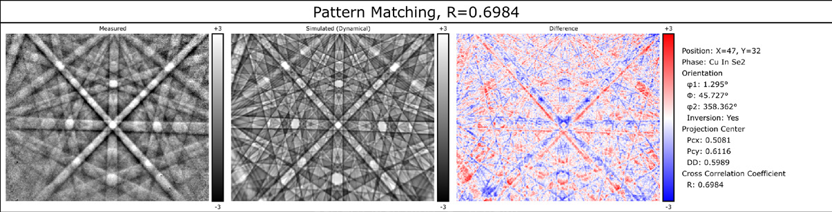
Result of pattern matching refinement for a single Cu(In,Ga)Se2 EBSD pattern using AZtecCrystal MapSweeper, resolving the true tetragonal orientation with a high normalised cross correlation coefficient (R = 0.6984).
Results
The original Hough-based indexing in AZtec could not reliably resolve the tetragonal structure of the Cu(In,Ga)Se2, resulting in a mix of 3 orientations in the CIGS layer as shown in the orientation map below. The lack of precision in this analysis is also clear in the Kernel Average Misorientation (KAM) map, highlighting local orientation changes of the crystal lattice (and therefore the presence of dislocation structures).
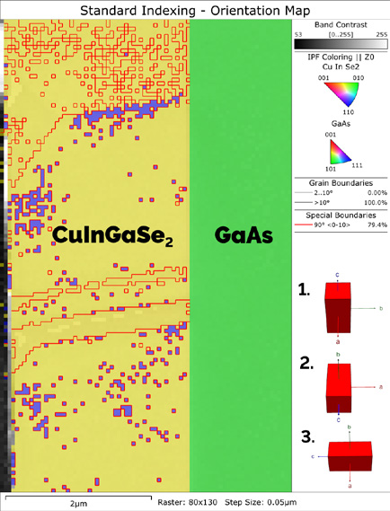
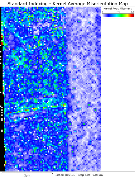
EBSD results from conventional Hough-based indexing. Left – orientation map with the CIGS thin film on the left side, with the sample surface at the left edge. Note the 3 different orientations (graphically illustrated by the 3D unit cell displays) due to the pseudo-cubic crystal symmetry. Right – KAM map, suggesting greater lattice distortion in the CIGS layer without resolving any individual dislocation structures.
Following the Refinement sweep in MapSweeper, the true tetragonal orientation of the CIGS layer has been resolved, as shown below. X-ray diffraction analyses indicate that this orientation is linked to the Ga:In ratio (or the "GGI" value – Ga/(Ga+In)) in the thin film and so the improved measurements using MapSweeper enable this relationship to be tested. The significant improvement in angular precision is apparent in the KAM map; unlike in the conventional EBSD data, the MapSweeper refined data clearly show the presence of clear dislocation structures associated with antiphase domains.
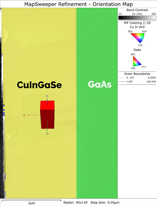
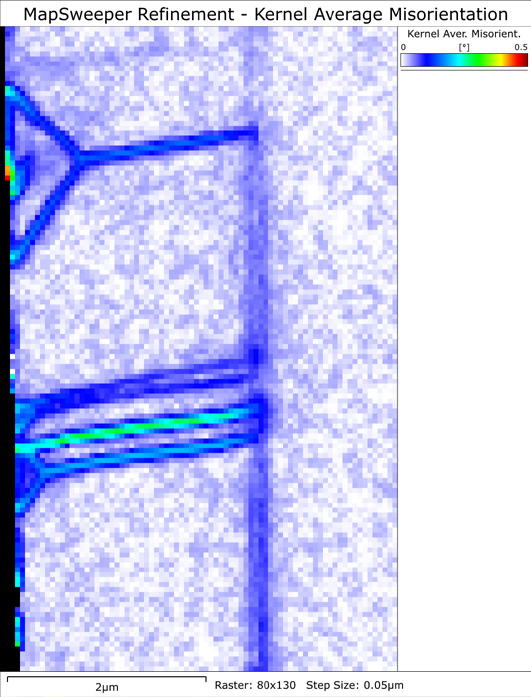
EBSD results following processing using AZtecCrystal MapSweeper. Left – orientation map, resolving the true tetragonal orientation of the CIGS layer, with the <100> direction normal to the sample surface. Right – KAM map (using the same 0.5° scale as for the conventional EBSD data results) highlighting clear dislocation structures associated with antiphase domain boundaries.
Summary
The refinement of EBSD data from a CIGS solar cell using AZtecCrystal MapSweeper has revealed the true tetragonal orientation of the crystal lattice and highlighted the presence of dislocation structures associated with antiphase domain boundaries. These were not visible following conventional EBSD analyses and demonstrate the power of hybrid pattern matching techniques within MapSweeper to reveal key microstructural features in such thin films, with corresponding implications for the optoelectronic performance of the material.
Acknowledgements
Oxford Instruments NanoAnalysis acknowledge Dr. Jiro Nishinaga (National Institute of Advanced Industrial Science and Technology (AIST), Japan) and Dr. Daniel Abou-Ras (Helmholtz Centrum, Berlin) for providing the sample and assisting with data interpretation.

