Published: 04 Oct 2022 · Last updated: 29 May 2026
Tags: 2D materials, AFM, Atomic Force Microscopy, electrostatic force microscopy (EFM), graphene, Kelvin probe force microscopy (KPFM)
Research Focus
What do nanomaterials such as 2D crystals and biomolecules have in common? Their atomic scale electric polarization properties can produce important macroscopic effects. And these effects can impact applications ranging from neuroscience and molecular biology to advanced photonic and energy storage devices.
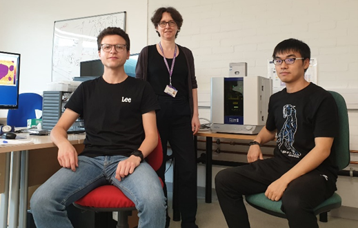
Dr. Laura Fumagalli of the Condensed Matter Physics Group, University of Manchester, is known for developing Scanning Dielectric Microscopy, a technique that can probe the dielectric properties of materials at the nanoscale based on atomic force microscopy (AFM) measurements of electrostatic force and current. In 2021, she needed a state-of-the-art AFM to expand her group’s measurement capabilities. Her most important criterion was getting atomic resolution in all three dimensions. She also wanted mode flexibility and sample environmental control, including simple operation in liquids.
“Our new Cypher ES AFM makes it so much simpler to achieve atomic-scale resolution, whether operating in air or in water.”
— Dr. Laura Fumagalli, Reader in the Condensed Matter Physics Group, University of Manchester, UK.
Research Methods
In her research, Laura makes extensive use of electrostatic force microscopy (EFM) to probe the dielectric properties of diverse materials under the influence of a voltage bias. For example, she used EFM to study interfacial and confined water [i]. Through this work, Laura and her co-authors clearly showed for the first time that water next to a surface is much less polarizable than in bulk water. This finding has important implications in multiple fields, from biology to energy storage technology. Low-noise electronics in the AFM was crucial here for maximizing the signal to noise in the data. Previously, she also used EFM to study the dielectric properties of biological molecules such as DNA and protein complexes [ii].
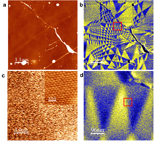
Laura is particularly active in the field of 2D nanomaterials, given her affiliation with the Graphene group and the National Graphene Institute in Manchester. For example, she recently studied 2D heterostructures, including 2D twisted layers, which have new electro-optical properties that could be used to develop next-generation devices [iii, iv]. In these studies, she and her group used both EFM and kelvin force probe microscopy (KPFM) to visualize ferroelectric and piezoelectric properties, in particular ferroelectric triangular domains in 2D twisted crystals shown below.
Examples of images taken with the Cypher ES on twisted bilayer of MoS2 by Laura and her group. Using electrostatic force microscopy (EFM), they observed ferroelectric triangular domains (b,d), not visible in the topography image (a). Lateral force AFM images in (c) enables visualization of the atomic structure of the layers (zoom in the squared region in indicated in (d).
User Impressions
Laura states that the Cypher ES Environmental AFM turned out to be an ideal choice for her lab: “First off, it definitely brings the high resolution we need in our work. And just as important, it’s reasonably easy to get this resolution on a regular basis with no special skills or touch required – even our less experienced students can take publication-quality data without much training.
“Plus, Cypher supports all the different modes we want, from simple morphology under air to the more challenging nanoelectrical measurements in different ambient conditions – like water-immersed samples. And we really value that the operating software is open-source. I’m always looking to optimize and extend AFM modes to interrogate samples in greater detail, so being able to use customized code is invaluable there.”
References
See for example
[i] L. Fumagalli et al., Anomalously low dielectric constant of confined water, Science 360, 1339–1342 (2018). https://www.science.org/doi/10.1126/science.aat4191
[ii] A. Cuervo et al., Direct measurement of the dielectric polarization properties of DNA, PNAS, E3624–E3630 (2014). https://doi.org/10.1073/pnas.1405702111
[iii] P Ares et al. Piezoelectricity in monolayer hexagonal boron nitride Adv. Mater. 32 (1), 1905504 https://onlinelibrary.wiley.com/doi/full/10.1002/adma.201905504
[iv] C.R. Woods et al., Charge-polarized interfacial superlattices in marginally twisted hexagonal boron nitride, Nature Comm., 12, 347 (2021) https://doi.org/10.1038/s41467-020-20667-2