Aim
Metallisation is an indispensable process in the manufacture of modern semiconductor devices. It connects different components together and directly affects the device performance. The occurrence of defects in metal layers will directly influence the performance of the device.
Challenge
If the metal layer is oxidised, resistance will increase and the electrical connection will be compromised, which will cause the performance of the device to deteriorate or even fail. Therefore, once a metal layer defect is found, failure analysis is crucial to find the cause of the defect and trace it back to the manufacturing process.
Solution
A large-area Ultim Max 170 EDS detector is ideal for the failure analysis of semiconductor devices. Its large x-ray detection area means that it is possible to work at significant throughput rates even when reducing SEM energy in order to reach the spatial resolution required for imaging/mapping components of this type. The acquired data is processed in the AZtecLive software, which includes Tru-Q® technology to ensure that true elemental distributions are determined.
Results
The sample shown here is a failed power device. A crack in an Al metal layer is obvious from an SE image, but the EDS map adds additional information by showing O incorporation - indicating oxidation. It is also clear that the Ti/TiN layer around the Al is discontinuous, whereas Cl and F exist at/above the Al layer. It is thus concluded that the photoresist and removal solution were not completely eliminated during manufacture. During the subsequent high temperature treatment, the photoresist corroded the Ti/TiN dielectric layer and diffused into the Al, which further resulted in the oxidation and chlorination of the metal, eventually leading to the generation of voids. The SmartMap shows F distribution throughout the analysis area, which can be misleading in finding the failure cause, but TruMap can eliminate the influence of the background and output the true element distribution, showing F ubiquitously distributed in the ROI.
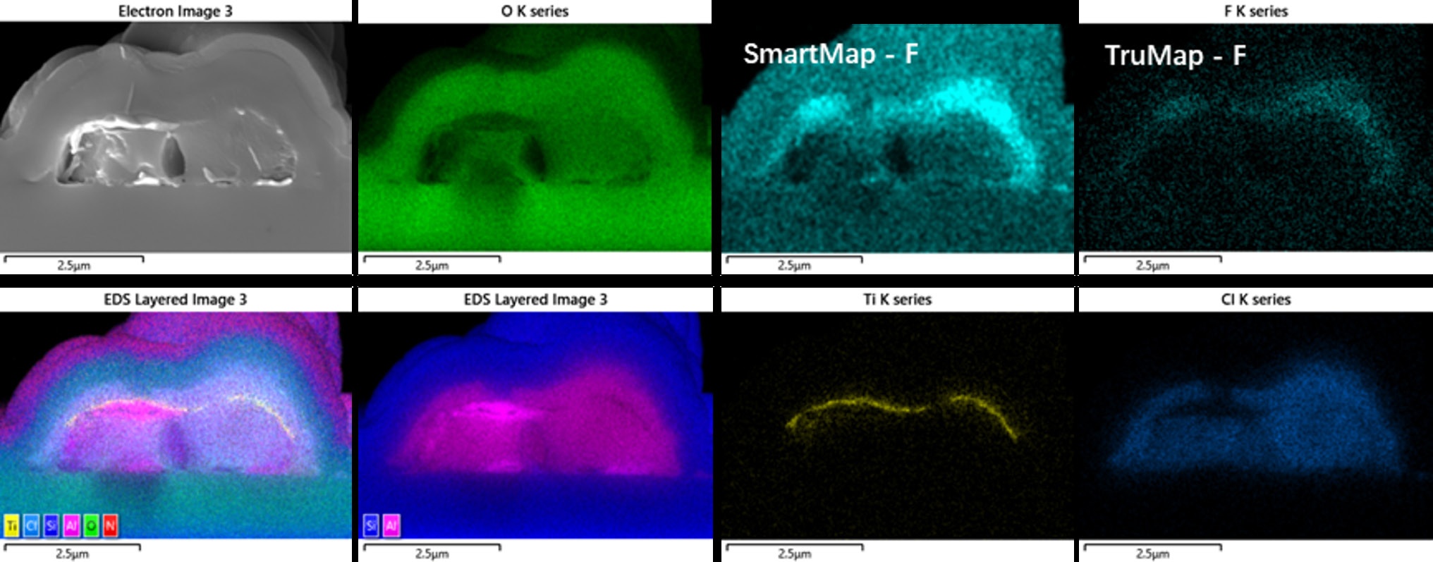
Figure 1. Cross section of the Power Device showing the failure site (Al Metal). Top left corner: F maps- SmartMap without removal of the of the background influence and TruMap showing the real F distribution
Conclusion
The results show how the combination of a large area Ultim Max 170 EDS detector with AZtecLive software, incorporating Tru-Q technology, is a powerful solution for finding the root causes of failure in power devices.

