Tags: AFM, Atomic Force Microscopy, conductive AFM (CAFM), EDS, Fast Force Mapping Mode, Scanning Probe Microscopy, SPM, tapping mode
Researchers characterized electrical conductivity, doping level, and physical properties on the nanoscale in pristine and electrochemically doped conjugated polymers. They found that dopant sites were concentrated in crystalline domains, leading to higher conductivity in these areas.
 Replacing inorganic semiconductors with conjugated polymers could enable low-cost solar cells, faster computers, and much more. Research has found that electrical conductivity in conjugated polymer films improves with relative crystallinity, and that molecular doping increases it even more. However, understanding is limited of how dopants are distributed between amorphous and crystal domains.
Researchers at Rutgers University investigated how local domain properties affected electrical properties of pristine and electrochemically doped films of poly(3-hexylthiophene) (P3HT). They characterized the physical, mechanical, and optical properties at the nanoscale using AFM, x-ray, and other techniques.
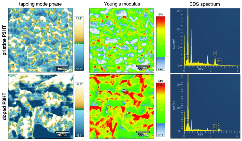
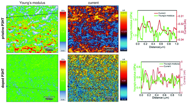
Nanomechanical images revealed crystalline and amorphous regions in both pristine and doped films, while nanoelectrical characterization showed that doped films conducted about 30 times more current than undoped ones. Combined analysis of these results and ones from Raman and energy dispersive x-ray spectroscopy (EDS) measurements indicated that dopants were concentrated in crystalline domains, which had much higher conductivity than amorphous areas.
The study offers insight into how the electrical properties of doped conjugated polymer films could be tuned at the nanoscale. In this way, it may help optimize these materials for use in next-generation electronic and optoelectronic devices.
Instruments used
Cypher ES with the Dual Gain ORCA module (AFM); X-Max 80 Silicon Drift Detector (EDS)
Techniques used
Multimode AFM characterization of P3HT films was performed on a Cypher ES AFM. Topography and phase images were acquired in tapping mode. Nanoscale maps of Young’s modulus and current were acquired in Fast Force Mapping and Fast Current Mapping modes, respectively. By acquiring high-speed arrays of force curves, these modes minimize tip wear and damage to delicate samples that scanning in contact can incur. Current imaging and point current-voltage (I-V) measurements used a Dual Gain ORCA module and cantilevers with conductive tips. The Dual Gain ORCA has two separate amplifiers, enabling conductive AFM (CAFM) measurements over a very wide current range (~1 pA to 10 µA). EDS spectra were acquired with an X-Max 80 Silicon Drift Detector by Oxford Instruments NanoAnalysis (since upgraded to Ultim Max) coupled to a field-emission scanning electron microscope.
Citation: H. Maddali, K. House, T. Emge, and D. O'Carroll, Identification of the local electrical properties of crystalline and amorphous domains in electrochemically doped conjugated polymer thin films. RSC Adv. 10, 21454 (2020). https://doi.org/10.1039/D0RA02796K
Note: The original article featured above was published as Open Access under a Creative Commons license. The data shown here are reused under fair use of the original article, which can be accessed through the article link above.

