The semiconductor industry fabricates integrated circuits and microchips that are used in a myriad of applications from communications to data processing and automotive sectors. To improve device performance and reduce cost, advanced manufacturing techniques and new technologies are being continuously developed. Semiconductor fabrication requires extreme level of cleanliness, as any contamination may result in device failure. For this reason, great care is taken to identify contamination and defects, and eliminate their sources. Quick and accurate identification of these sources coupled with feedback into the manufacturing process can help ensure a stable supply of products and increase profitability through yield improvement.
Many of the advances in semiconductor devices result from the ever-shrinking "technology nodes," which relate to the smallest features in the devices. Over just the last 20 years, feature sizes have been reduced by a factor of ten, from >100 nm features to <10 nm features. While smaller means cheaper and faster, miniaturisation also means that particles and defects of smaller size can have large effects on the devices and must therefore be controlled.
For example, when photomask blanks used for extreme ultraviolet lithography (EUV) processes are produced, the goal is to reduce the number of particles larger than ~20 nm, on a 6-inch photomask blank, to zero. Initial contamination inspection is done using light scattering to locate defects, but it cannot provide accurate information about defect type (i.e. particle vs. indent). To further study the contamination, scanning electron microscopy coupled with energy dispersive X-ray spectroscopy (SEM/EDS) could be used, but it is difficult to analyse such small-sized particles using SEM. The other technique that can be used is transmission electron microscopy (TEM/EDS).
To perform TEM analysis efficiently, the type of contamination should be identified (particle or defect) and its exact location confirmed. Atomic force microscopy (AFM) has become an indispensable tool used to easily identify very small contaminates and indicate if the contaminate is a particle, a hole defect, or a bump, while providing the exact defect location.
The Jupiter Discovery AFM from Oxford Instruments (Figure 1) has several features that set it apart from conventional AFMs, thereby making it the instrument of choice for contamination detection and analysis.
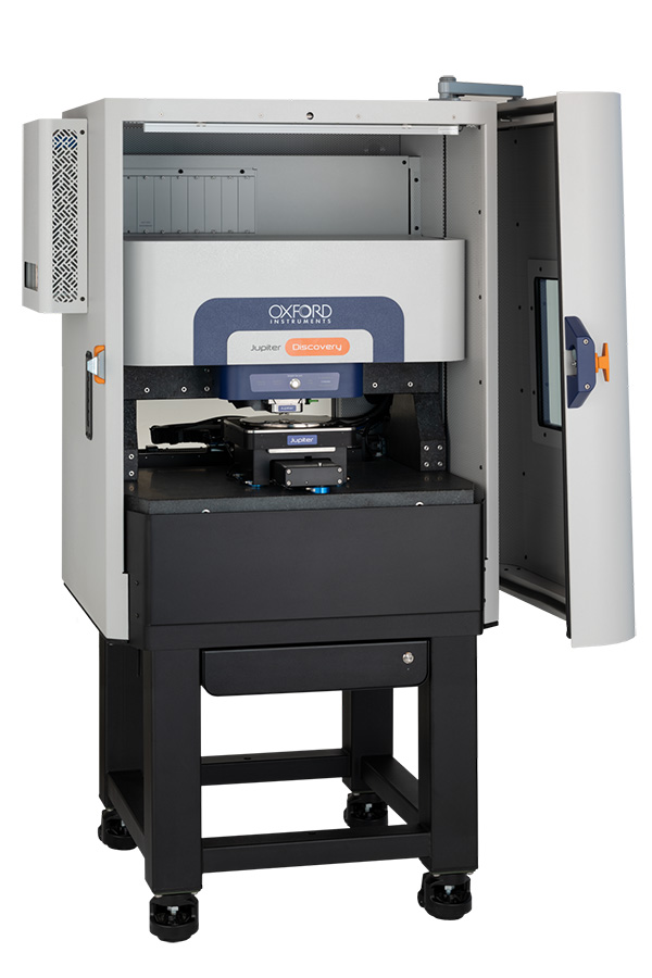
Figure 1: Jupiter Discovery large-sample AFM
The Jupiter Discovery AFM uses Oxford Instruments' exclusive blueDrive photothermal tapping mode that ensures that the quality of data is accurate and repeatable. Most importantly, the Ergo software has 3-point alignment and coordinate correction functions that facilitate particle localisation (Figure 2).
The Jupiter Discovery AFM can scan large areas of the sample (up to 100 µm) with high pixel count to detect nanometer-sized particles or defects. At a conventional image pixel count of 512×512, each pixel in a 100 µm image measures almost 200×200 nm square. However, at a higher pixel count of 4096×4096 pixels, each pixel represents an area of only about 2.5×2.5 nm square.
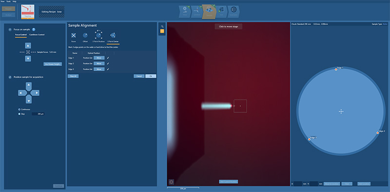
Figure 2: Ergo software interface showing 3-point alignment using fiducial markers
Additionally, imaging on a Jupiter Discovery AFM is performed rapidly such that a high pixel count image, comparable to the one shown in Figure 3C (20 µm image with pixel size of 20×20 nm), can be obtained in under 2 minutes which is an important consideration for industrial productivity.
Furthermore, Ergo has automation and Autopilot functions. Automation enables the AFM user to collect data at multiple sites (up to 1,000 sites) without requiring user interaction, whereas Autopilot is an advanced algorithm which determines optimal imaging parameters automatically to make the data collection simple for every AFM user.
All these features, coupled with the low noise of the Jupiter Discovery AFM, means the detection of nanometer-sized defects and particles can be done with speed and accuracy surpassing any other AFM.
An example of a particle contamination measurement is shown in Figure 3. The sample has been first analysed using a scattering technique and the general area where contamination was found was marked with optically visible indents. The indents are visible in the AFM video camera view (Figure 3A) and are used as reference marks to determine the area to be imaged by AFM. A survey scan of 30 µm was acquired and included the 3 indent reference points (Figure 3B). A slightly smaller image of 20 µm with a much higher pixel count (Figure 3C) was acquired inside the area bordered by the indents, in order to locate the contamination that was first detected by a light scattering technique. The image clearly showed contamination, specifically a particle that, when imaged more closely (Figure 3D), appeared to be an irregularly shaped particle 250 nm in size.
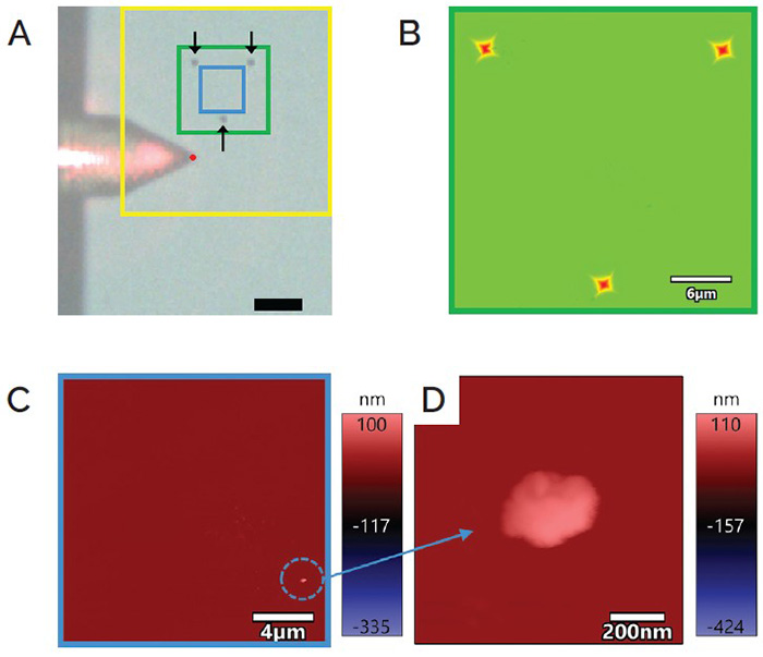
Figure 3: Localisation and imaging of sample contamination using a Jupiter AFM. a) Optical view of the sample showing indents (arrows), the AFM tip (red dot), and the outlines of the different scan areas for reference: 20 µm (blue), 30 µm (green), 100 µm (yellow). Scale bar is 20 µm. b) AFM image showing the 3 indents visible in optical image. c) AFM image of the area where the contamination was detected. d) Zoom-in into the contamination area showing a particle of ~250 nm in diameter.
In summary, characterisation of this sample with an Oxford Instruments Jupiter AFM provided information about the type of contamination present, an irregularly shaped particle, as well as its exact location on the sample. The particle's position coordinates can now be used to further analyse it using SEM/EDS or TEM/EDS techniques.
The Jupiter AFM has become an indispensable tool for defect inspection used to accurately identify and provide the exact location of nanoscale contaminates with high speed and accuracy.

