Products
DEPOSITION TOOLSPlasma Enhanced Chemical Vapour Deposition (PECVD)Inductively Coupled Plasma Chemical Vapour Deposition (ICPCVD)Atomic Layer Deposition (ALD)Ion Beam Deposition (IBD)ETCH TOOLSInductively Coupled Plasma Etching (ICP RIE)Reactive Ion Etching (RIE)Deep Silicon Etching (DSiE)Atomic Layer Etching (ALE)Ion Beam Etching (IBE)
Learning


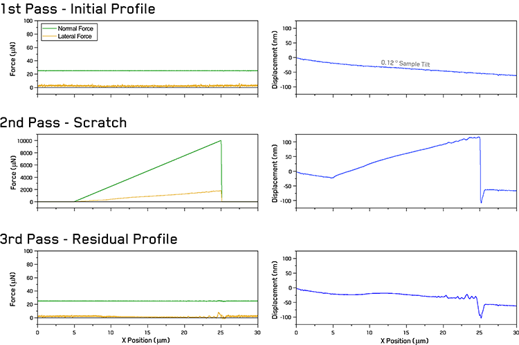 Figure 1. Illustration of a 3-pass scratch procedure showing the forces and displacements measured during the 1st initial profiling pass, the 2nd ramped-load scratch pass, and the 3rd residual surface profile pass.
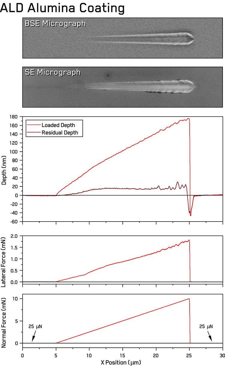
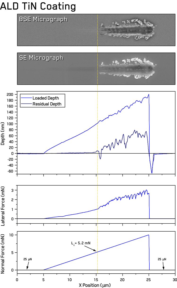
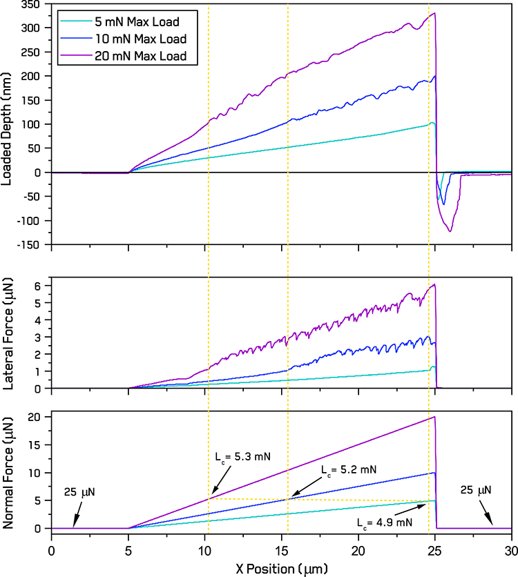 Figure 4. Scratch forces and loaded depth vs. position during progressive scratches to different maximum loads on 60 nm thick ALD alumina on Silicon with variation in critical load marked.