Mechanical microscopy allows the imaging of mechanical property variations at multiple length scales. Nanoindentation mapping is usually performed at the microstructural length scale, but many manufacturing processes create property variations on larger scales, e.g. case hardening, nitriding, or designed variations through additive manufacturing. In this series of application notes, we demonstrate how mechanical microscopy can be performed at multiple length scales to connect large-scale variations in mechanical properties to their mechanical properties on a microstructural length scale. This demonstrates the wide range of measurements possible with Oxford Instruments Nanoindentation systems. In this second note, we study the application of nanoindentation mapping over three orders of magnitude in length scale on a case-hardened medium carbon steel. This application of mechanical microscopy to measure property variations from the meso- to the micro-scale demonstrates the true multi-scale capability of the technique.
Introduction
Mechanical microscopy allows the imaging of mechanical property variations, such as hardness and reduced elastic modulus, over a sample’s surface. This is typically performed at the microstructural length scale using nanoindentations with depths on the order of 100 nm. However, mechanical microscopy is truly a multi-scale technique, which allows spatial resolution from the sub-micron scale up to the millimeter or centimeter scale. This is very useful for the study of materials resulting from manufacturing processes that generate both large and fine-scale property changes such as case hardening, nitriding, or designed variations through additive manufacturing.
As introduced in the previous note in this series, case hardening is a well-known surface treatment for steels that hardens the surfaces of parts through heat treatments that induce phase transformations from soft, ductile Ferrite to hard, brittle Martensite.
In this application note, we demonstrate the ability of multi-scale Mechanical Microscopy to characterize both the large-scale property variations and the fine-scale microstructural features within such a material. This is technically challenging to achieve and requires a combination of displacement control and multi-scale load ranges. In the next and final note in this series, we combine these measurements to show the length-scale variations in the each of the phases in the material.
Experimental Considerations
Sample Manufacture
A sample of medium carbon C45 steel (1.0503) was induction hardened at 850 °C and tempered at 210 °C to generate a case-hardened layer. The sample was metallographically investigated by sectioning, polishing, and etching with alcoholic nitric acid ~ 3% (Nital) to reveal the underlying microstructure. The sample was then repolished for indentation by using successively finer media to a final polish with a 50 nm alumina suspension.
Multi-scale Measurement
To perform measurements with maximum resolution over a range of length scales, the inter-indentation spacing needs to be held constant [1]. This requires displacement control to ensure consistent indentation size, and a wide range of load capacity to accommodate both hard and soft phases within the region.
|
Sensor
|
Force Range
|
Resolution
@ 10 Hz
|
|
FT-S2,000
|
±2,000 µN
|
0.005 µN
|
|
FT-S20,000
|
±20,000 µN
|
0.05 µN
|
|
FT-S200,000
|
±200,000 µN
|
0.5 µN
|
|
FT-S2,000,000
|
±2,000,000 µN
|
5 µN
|
Table 1. FT-S Microforce probe specifications.
This is a basic requirement to perform the measurement, as a 2.5 µm deep indentation in Martensite requires over a Newton of force, while a 25 nm indentation into Ferrite may need only a few tens of µNs. Oxford Instruments Nanoindentation systems offer a range of sensors with ranges from millinewton down to sub-nanonewton forces - Table 1.
Nanoindentation Mapping
Nanoindentation maps were performed at a range of different length scales using an i04 Femto-Indenter with a diamond Berkovich indenters mounted to several different sensors, as appropriate for the desired force range, e.g. an FT-S2,000,000 for the largest indentations and an FT-S2,000 for the finest scale.
At the larger scales (Figure 1), indentations were performed in neighboring rectangular grids of 3600×100 µm with four different indentation depths/spacings at semi-log intervals: 25, 10, 5, and 2.5 µm spacings. An indentation depth/spacing ratio of 10 was maintained [1], so the maximum depths are always 1/10th of the spacing. In all indentations, the continuous stiffness measurement (CSM) method [2] was employed in displacement control, and representative values for each indent were taken by averaging values from depths >80%hmax to minimize the influence of indentation size effects for hardness values and >50%hmax for modulus values.
At the finer scales, indentations grids were performed in square grids 100×100 µm with three different indentation depths/spacings at semi-log intervals: 1, 0.5, and 0.25 µm spacings. These grids were located within the center of the Martensitic and Pearlitic regions at distances of ~600 and 2800 µm from the sample edge, respectively.
Results and Discussion
As in the previous application note, indentation maps are presented with an optical micrograph of the etched microstructure of the sample for visual comparison. Mechanical microscopy results for hardness and modulus are shown for the long meso-scale maps on this case-hardened C45 steel sample are shown in Figure 1.
The optical micrograph of the etched cross-section reveals the microstructural transitions undergone by the C45 steel during case hardening. The outer portion of the steel on the left has been transformed into Martensite. Moving towards the right, a transition region is observed with a mixture of Martensite and Ferrite. Finally, the microstructure of the medium-carbon steel is observed with Pearlite showing its namesake rainbow colors interspersed with white Ferrite.
The meso-scale nanoindentation maps appear in Figure 1 as long rectangles of measured properties with increasing resolution as the indentation spacing is decreased. At 25 µm spacing, the lateral resolution only allows for 5 indentations across the 100 µm, and this relatively coarse resolution only allows the overall trend in hardness to be observed. In hardness, the Martensite and Pearlite regions appear relatively uniform with a smooth transition between them, while the reduced modulus appears more consistent in the Martensitic region.
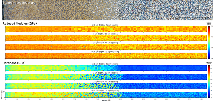 Figure 1. Meso-scale hardness and reduced modulus variation over case-hardened C45 steel in cross-section – Optical micrograph showing the etched microstructure and indentation maps performed at 4 different indentation depths/spacings. As the indentation size is decreased, the resolution increases, revealing additional microstructure features.
On increasing the resolution (decreasing the indentation size/spacing), we begin to more clearly visualize the variation in hardness between the different phases. In the Pearlitic region, regions of higher hardness Pearlite and low hardness Ferrite become distinct. While in the Martensitic region, the modulus appears to show much finer-scale features, compared to the larger islands of harder regions.
At first glance, the 2.5 µm spacing micrograph in Figure 1 appears to completely capture the local microstructure variations. However, deeper investigations at the micro-scale, shown in Figure 2, reveal that there is still more to see. In the Martensitic region, the 1 µm spacing maps first reveal the presence of untransformed Ferrite islands within the Martensite, which correspond to the bright islands seen in the etched microstructure. On decreasing further to 0.5 µm spacing, the needle-like acicular structure of the Martensite is revealed. This becomes even clearer at 0.25 µm spacing.
In the Pearlite region, the microstructural differences in results with increasing resolution are even more spectacular. At 1 µm spacing, the Ferrite and Pearlite regions are clearly resolved. However, by 0.5 µm spacing, fine-scale variation within the Pearlite becomes apparent. At 0.25 µm spacing, this is revealed to be the result of individual plates of Cementite within the Pearlite! This demonstrates the comprehensive ability of multi-scale mechanical microscopy to reveal mechanical property variations from the meso- to microstructural length scale.
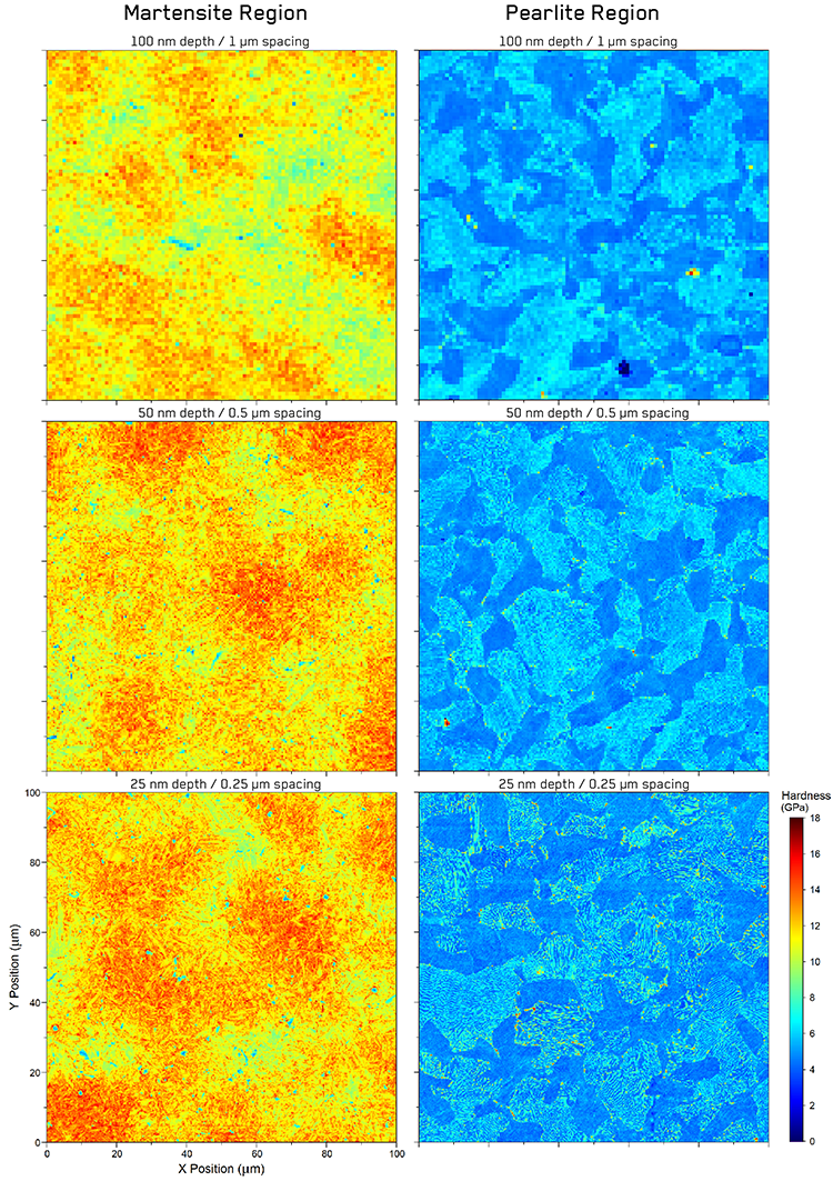 Figure 2. Micro-scale hardness maps acquired in the Martensite and Pearlite regions of the sample at three different depth/spacing increments.
Conclusion
In this application note, the capability of mechanical microscopy to image mechanical property variations over three orders of magnitude in length scale was successfully demonstrated across a case-hardened C45 steel cross-section. Meso-scale maps over the entire heat treated region were able to clearly resolve the phase-level properties of the Martensite, Pearlite, and Ferrite grains with good agreement to optical microscopy. Maps performed at the microstructural length scales were able to probe even further and reveal the local morphology of the acicular Martensite and individual lamella of Cementite lamella within the Pearlite grains. This was only possible through both displacement control to achieve consistent sizes and spacings and the wide range of force sensors spanning several orders of magnitude. This application of mechanical microscopy to measure local property variations at both the meso and microstructural length scales, even for sub-micro features.
References
- P.S. Phani, W. Oliver, Materials & Design, 164 (2019) 107563.
- W.C. Oliver, G.M. Pharr, Journal of Materials Research, 7 (1992) 1564-1583.

