Defects and impurities in solar cell materials have a huge impact on the efficiency of the final product, acting as recombination centres for charge carriers. The main defects in multicrystalline Si affecting performance are point defects (e.g. particulate impurities), linear defects (dislocations) and planar defects (e.g. grain boundaries). Despite a long history of investigations on these defects there are still significant gaps in our knowledge of how the crystallographic nature and impurity decoration at these defects impact their electrical activity.
This note describes a simple method of preparing and analysing crystallographic defects in silicon on the nano-scale using Electron Beam Induced Current (EBIC), followed by sample preparation for atomic scale analysis techniques such as Transmission Electron Microscopy (TEM) and Atom Probe Tomography (APT).
Introduction
The use of solar cells is increasing worldwide and a wide range of semiconductor materials have been shown to be suitable for the active layers that convert sunlight into electric charge. However, the number of materials that can be manufactured economically while at the same time providing sufficient conversion efficiency and a long life time is relatively small. Solar cells manufactured from multicrystalline silicon (mc-Si) are cost effective and durable compared to other competing technologies and account for more than half of all industrial and domestic photovoltaic installations. Recent advances have led to industrial champion mc-Si cell efficiencies of over 21%, however typical industrial cell performance is much lower, in large part due to variability in the distribution of recombination centres between mc-Si wafers. These recombination centres include impurity decorated grain boundaries and dislocations, and act to reduce the efficiency of the solar cell by reducing the number of light generated minority carriers which are collected at the p-n junction. As such, an understanding of these defects – the elements which decorate them, their recombination activity and what processes can reduce this activity, is essential if improvements are to be made.
Established Investigation Methods
The dominant methods to image carrier lifetime and recombination in silicon solar cells are photoluminescence (PL) imaging and electroluminescence (EL) imaging. Both PL and EL imaging can be used to image defects in solar cells on a macro scale, and are widely used for in-line quality inspection of whole solar cells modules. However, when measuring dislocations, imaging resolution on the nanoscale is required as a dislocation is defined by a single missing atomic plane in the material. PL is an optical technique and its resolution is usually limited to the microscale. EL type measurements can in theory provide nanoscale resolution but they need electrical contacts and a closed circuit to be established and are therefore mainly used on finished solar cell modules.
Here we show how such defects can be analysed using EBIC with an electrically enabled nanomanipulator to enable extremely highly spatially resolved direct imaging using the charge carriers generated by the electron beam. We also show how such regions can be easily lifted out for subsequent analysis using TEM and APT.
EBIC Enabled Manipulator
Electron Beam Induced Current (EBIC) is an SEM/FIB based technique which utilizes an incident electron beam to induce currents in semi-conductor samples. As the beam is scanned over the sample the generated current will vary with the structures that are scanned. This variation can be detected and measured by connecting the sample to an amplification system which is able to associate the current with the beam position to produce images where the contrast indicates the degree of current flow. In this application this enables imaging of recombination activity of dislocations as illustrated on Figure 1.
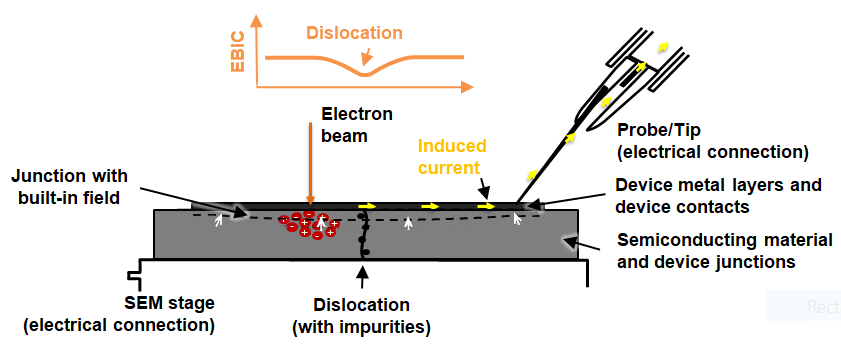
Fig. 1 - EBIC signal generation in Solar cell material.
Here we present a method which utilizes a nanomanipulator which has been combined with an EBIC system to both identify dislocations and lift out samples for subsequent analysis. By using the same nanomanipulator for both the EBIC characterization of the sample and lift-out of dislocations, handling is reduced and workflow speed and ease is greatly improved. Capital expenditure on equipment is also reduced as only one piece of equipment is needed for both tasks. The identification and lift-out of a dislocation can be achieved in a single analysis session.
Sample Preparation and Experimental Method
P-type mc-Si samples were prepared through polishing of the surface to be imaged. This was followed by a defect revealing etch (in this case Secco) to reveal dislocations and grain boundaries through the formation of etch pits. It is important that these etch pits have a high aspect ratio such that they are clearly visible in the SEM for defect marking, but do not obscure a significant fraction of the EBIC image around the defects. The samples were then RCA cleaned and 13 nm of aluminium was thermally evaporated on the front surface to form a Schottky contact. The samples were then mounted on a sample stub using indium-gallium and silver dag to provide good ohmic contact between the rear surface of the sample and the FIB stage. The stage and nanomanipulator (OmniProbe 200) (fitted with a coaxial shaft) were connected to the EBIC amplifier (Oxford Instruments/Point Electronic DISS5 system). Whilst imaging with the e-column, the nanomanipulator was placed on the Schottky contact, creating the setup shown in Figure 1.
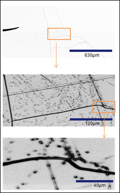
Scanning the electron beam across the sample at different magnifications provides a solution which can give information over a larger range of length scales from mm to nm, as shown on Figure 3. While the etch pits are clearly visible on the images it is also possible to observe the recombination activity associated with the dislocations.
Results
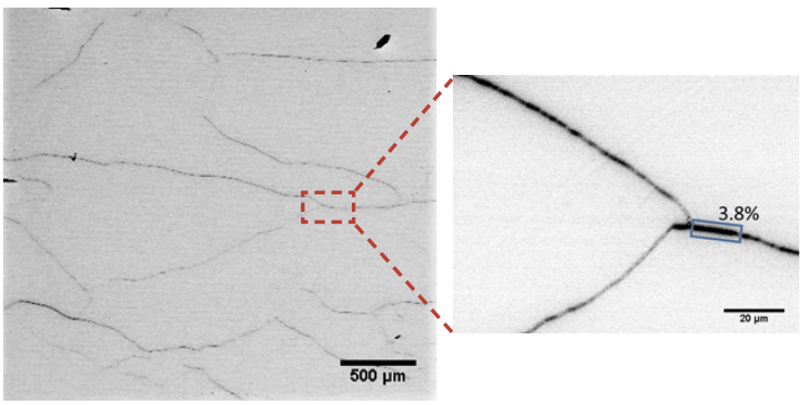
Fig. 2 - EBIC used to identify grain boundary recombination activity
It was noted from Figure 2 that some defects had a significantly higher EBIC contrast than others. It is this difference that is of particular interest for further study. Several defects were chosen for further analysis. The etch pits make location and selection of these defects straightforward as they can be observed in SEM mode and filled with tungsten using a gas injection system. A carbon protection layer was also deposited. A trench was then milled around the sample to create a lamella. This was then lifted out with the nanomanipulator and attached to a TEM half grid, as shown on Figure 3. Once mounted it is then available for further high resolution structural analysis using techniques such as transmission electron microscopy or atom probe.
Conclusion
Mc-Si solar cells offer an important solution for future energy sources, however production improvements are required in order for this material to reach its full potential. These improvements are dependent on an understanding of nano scale features within the solar cell. We have presented a means of analysing samples on both the nano and atomic scale, enabling a multiscale analysis of solar cell performance, correlating impurity decorated dislocations to their electrical activities.
The OmniProbe nanomanipulator offers a single solution for EBIC and liftout, improving the workflow and cost. Its ease of use and high operating precision significantly reduces the likelihood of failure due to lost samples.
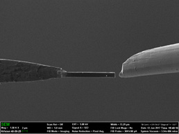
Fig. 3 - The lifted out lamella after attachment to a TEM half-grid. The selected defect appears as a white spot on the visible face of the lamella.
Acknowledgements
With thanks to David Tweddle, Peter R Wilshaw and Phillip Hamer of Oxford University* who conducted this research and made major contributions to this application note.
* University of Oxford, Department of Materials, Parks Road, Oxford, OX1 3PH, UK

