Mechanical microscopy allows the imaging of mechanical property variations at multiple length scales. Nanoindentation mapping is usually performed at the microstructural length scale, but many manufacturing processes create property variations on larger scales, e.g. case hardening, nitriding, or designed variations through additive manufacturing. In this application note, we demonstrate how mechanical microscopy can be performed at larger length scales to investigate these features. This is used to investigate the printed-in variation in mechanical properties created by a novel additive manufacturing process. This is only possible using an indentation system with a combination of high system stiffness, a high load range, and fast dynamics to allow rapid indentations to large depths. This application of mechanical microscopy to measure meso-scale property variations demonstrates the multi-scale property characterization capability of the technique.
Introduction
Mechanical microscopy allows the imaging of mechanical property variations, such as hardness and reduced elastic modulus, over a cross-section of a sample. This is typically performed at the microstructural length scale using nanoindentations with depths on the order of 20-200 nm. However, mechanical microscopy is truly a multi-scale technique, which allows spatial resolution from the sub-micron scale up to the millimeter or centimeter scale. This is simply accomplished by simply performing a either numerically large map of fine-scale indentations over a large area or by using larger indentations at proportionally greater spacings. By performing mechanical microscopy at the meso-scale, larger scale property variations resulting from manufacturing processes such as case hardening, nitriding, or designed variations through additive manufacturing can be measured.
Additive Manufacturing (AM) is a transformative technology which enables rapid fabrication of complex geometries previously inaccessible by traditional methods. However, some novel AM techniques allow not only complex geometries to be achieved; they enable site-specific properties to be tailored within the geometry, as well.
In this application note, we demonstrate the capabilities of Mechanical Microscopy to characterize meso-scale properties of an AM steel with site-specific properties printed into the material using a customized binder jetting system.
Experimental Considerations
Sample Manufacture
A customized HP metal printer was utilized in this study, which was equipped with a printhead system that can accommodate 2 different binders in separate slots at a spatial resolution of as high as 1200 dpi. The 2 binders used in this work are HP binding agent and a custom-made C-rich binder (CB), which is made from the HP binding agent additionally loaded with 5 wt% carbon in the form of nanoparticles.
To summarize the printing procedure, the platform is first moved down a distance of 1-layer thickness (60 μm), followed by the spreading of powder to form a new layer. The binder deposition is then executed at designed location. Immediately after that, the heat lamp is turned on and placed close to the powder bed surface for 30 sec. These steps are repeated for every layer until the part is completed.
A 2-stage sintering process was designed and employed to limit the C diffusion. The first stage consists of a 900 °C hold for 4 hr, followed by the second stage at 1300 °C for 1 hr. The sample was then solutionized at 850 °C for 30 min before water quenching.
The sintered part is cut to reveal its cross-section, hot-mounted, and mechanically polished to a mirror surface using progressively finer abrasives until a final polish achieved using a 50 nm alumina suspension.
CSM Indentation Procedures
Nanoindentation maps of 150×100 indents (Figure 1a) were performed on each sample using an FT-I04 Femto-Indenter (FemtoTools AG, Switzerland) with a diamond Berkovich indenter on a FT-S2,000,000 sensor. Each indentation was performed using a continuous stiffness measurement (CSM) method [1] in displacement control at a rate of 2 µm/s. Typical results from these indentations are shown in Figure 1. The indentations were each performed in ~1 s with an oscillation frequency of 150 Hz and an amplitude which was linearly increased from 2 nm to 10 nm, as shown in Figure 1. The total time for each indentation including repositioning was ~2.5 seconds.
Each indentation was performed to a specified depth of 5 µm, so that a spacing of 100 µm between indentations could be used while still ensuring an indentation depth/spacing ratio of 20 was maintained [3]. This avoids any significant interaction between neighboring indents. To achieve an area function at greater depths than fused silica allows due to cracking (> 2 µm), a hybrid method similar to Ginder and Pharr [2] was employed.
Hardness and reduced modulus were measured as a function of depth for each location, as shown in Figure 1, and representative values for each were taken by averaging values from depths >150 nm to minimize the influence of indentation size effects for hardness values and >100 nm for modulus values.
Electron micrographs were taken of each test region with a Zeiss EVO 25 scanning electron microscope (SEM) at 10 kV using a HD Backscattered Electron Detector (BSE).
System Sensitivity
High speed, regular maps of indentations are not useful unless the measurement sensitivity is high enough to resolve the variations within the mapped region. The measurement sensitivity is a function of several parameters: force and displacement noise floors, system dynamics, repeatability.
The primary influence on system’s measurement sensitivity is its noise floor in both force and displacement. For performing nanoindentation maps, tolerances in measurement noise must be very tight, particularly for identifying the contact point and during CSM measurements. As shown in the inset in Figure 1, each µN of noise counts in order to accurately determine the initial contact point. For indentations with a total depth of < 200 nm, each nanometer of accuracy will have an effect.
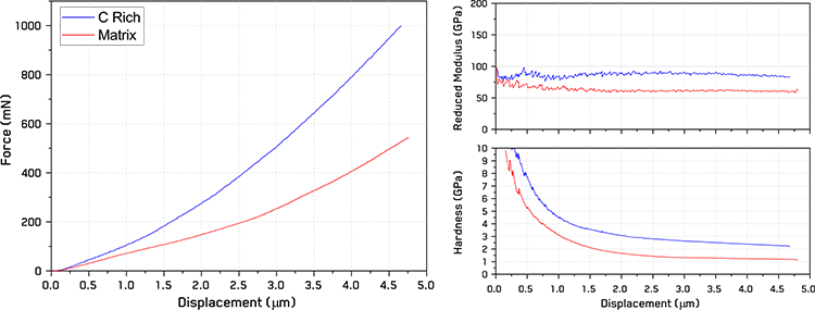 Figure 1. Typical indentation results for carbon rich and matrix regions of the sample.
Continuous stiffness measurements (CSM) allow the acquisition of many stiffness measurements to be acquired as a function of penetration depth during a single indentation. This is how hardness and reduced modulus can be measured as a function of depth during indentation. To prevent fatigue of the near surface [3] and accurately capture the indentation size effects, as seen in Figure 1, these oscillations should ideally be small relative to the indentation force and depth during the oscillation. This is why it is important that the initial oscillation amplitude is kept sub-nanometer, so that the force amplitude of the oscillation is also kept to a small fraction (in this case ~15%) of the total load.
Results and Discussion
To demonstrate the site-specific property control of this novel binder jetting technique, a sample was printed a sample in the design illustrated by the 3D schematic in Figure 2 using the HP metal 3D printer. The design consists of a martensitic “NTU” text (the acronym of Nanyang Technological University) embedded into a ferritic matrix. We produced the letters by jetting a carbon rich binder in 0.67 mm wide “strokes” and used the HP binding agent for the surrounding areas.
The hardness map shown in Figure 2 covers an area of 15 mm x 10 mm using 15,000 indents with a spacing of 100 μm. The grid of indentations can be seen to consist of a regular grid with uniformly sized indentations, despite the variation in properties and local porosity. The hardness map clearly highlights differences in local hardness, which are ~80% higher for the C-rich regions (~2.25 GPa).
In addition to the controlled hardness variation derived from differences in local composition and microstructure, Figure 2 clearly shows “waves” of hardness in the background region. These variations result from the presence of porosity defects, which likely stem from poor sintering due to uneven packing of powder particles during the re-coating of layers. This result proves the concept and demonstrates the efficacy of site-specific alloying during binder jetting 3D printing for material’s property tuning.
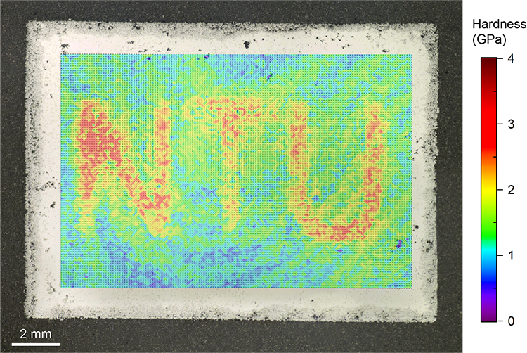 Figure 2. Meso-scale Hardness map of a sample with site-specific properties, which is superimposed to the optical micrograph of the polished sample surface. The schematic at the bottom right corner illustrates the 3D design of the sample.
Conclusion
In this application note, the capability of mechanical microscopy to image of mechanical property variations at the meso-scale was successfully demonstrated using an FT-S2,000,000 sensor. This allowed indentations to be performed to maximum depths of 5 µm at loads of up to 2 Newtons. This extends the effective imaging area from the order 100 µm2 to the order of several cm2. This enabled the investigation of the printed-in variation in mechanical properties in a sample created by a novel binder jetting additive manufacturing process. This application of mechanical microscopy to measure meso-scale property variations demonstrates the multi-scale property characterization capability of the technique.
Acknowledgements
We are grateful for the collaboration with the group of Prof. Matteo Seita at Nanyang Technological University (now at the University of Cambridge) which provided the sample for this application note. That work was supported under the RIE2020 Industrial Alignment Fund – Industry Collaboration Projects (IAF-ICP) Funding Initiative, as well as cash and in-kind contribution from the industry partner, HP Inc, through the HP-NTU Digital Manufacturing Corporate Lab. The full results from this collaboration are described in the following publication:
P-J Chiang, K.P. Davidson, J.M. Wheeler, A. Ong, K. Erickson & M. Seita, “Site-specific alloying through binder jet 3D printing,” Materials & Design (2023).
References
- W.C. Oliver, G.M. Pharr, Journal of Materials Research, 7 (1992) 1564-1583.
- R.S. Ginder, G.M. Pharr, Journal of Materials Research, 34 (2019) 1130-1137.
- M.J. Cordill, M.S. Lund, J. Parker, C. Leighton, A.K. Nair, D. Farkas, N.R. Moody, W.W. Gerberich, International Journal of Plasticity, 25 (2009) 2045-2058.

