High temperature microcompression is an exciting application that allows uniaxial stress-strain behavior to be measured as a function of temperature for site-specific microstructural features: grains with a desired orientation, grain boundaries, or secondary phases. However, it can be quite technically demanding as it requires a system capable of displacement control, high temperature operation, and in situ observation to facilitate the testing. In this application note, high temperature microcompression of lithography silicon pillars is demonstrated at temperatures up to 800 °C. This is the first observation of the deformation of micro-scale silicon in this temperature regime. Size effects at the highest temperature range appear to increase, suggesting significant high temperature strengthening may be achieved by reducing the scale of silicon components.
Introduction
High temperature microcompression is a powerful application of nanoindentation systems to perform uniaxial testing of small volumes at elevated temperatures. Microcompression testing was first introduced by Uchic et al. in 2004 [1], when they utilized a nanoindenter fitted with a flat-punch indenter to compress focused ion beam (FIB) machined micropillar samples. This was intended to allow uniaxial stress-strain behavior to be directly measured from small volumes rather than more complex
hardness values that arise from a triaxial stress state. This was successful along with the unanticipated discovery of the “size effect”, where small volumes display higher strength than their bulk equivalents. This led to many investigations into the nature
of the size effect in a wide range of materials [2], which is still an active area of research.
However, the combination of nanomechanical testing and FIB-machined micro-geometries has also yielded many other exciting avenues for research. The site-specific nature of FIB-machining allows individual microstructural features such as grain
boundaries, individual grains of selected orientations, inclusions, et cetera to be directly tested. Using pillar geometries, properties like compressive strength, critical resolved shear stress, and work hardening can be measured, and using other geometries
like dogbones or cantilevers can allow for properties like tensile strength and fracture toughness, respectively, to be investigated on individual microstructural features of interest. In many ways, a legacy of Uchic et al.’s combination of the FIB and nanomechanical testing has been the subsequent miniaturization of nearly every type of mechanical testing geometry to allow local mechanical properties of all types to be studied.
In addition to diverse loading cases, significant research has gone into developing these small-scale mechanical techniques for application under different environmental conditions, particularly high temperature. This is technically challenging [3], as the small
scale of nanomechanical measurements requires high precision control of temperatures and thermal gradients to prevent thermal expansion from interfering with the measurements. However, there are significant motivations to achieve such testing to
enable a wide variety of applications: operando testing at service temperatures, testing brittle materials above their brittle-ductile transition temperature, high temperature creep and fatigue testing, activation energy analysis of deformation mechanisms,
and studying thermally-activated phase transformations like in shape memory alloys.
In this application note, the experimental considerations and system requirements for high temperature microcompression testing are briefly described and discussed, particular the influences of control mode, high temperature operation, and in
situ testing. The application of these techniques to investigate the high temperature deformation of Silicon micropillars is then presented and discussed in relation to literature values from both micro-scale and bulk testing.
Experimental considerations
For a system to perform this application, several factors are important to consider: the accuracy of stress-strain measurement, the system’s high temperature operation, and in situ observational capabilities. Each of these factors can have a significant effect on the quality of the data, as well as the speed and ease of testing.
Stress-strain Measurement
The primary motivation for performing micro-compression testing rather than nanoindentation is the acquisition of uniaxial stress-strain behavior, rather than a hardness number arising from a complex stress state. To achieve this, the geometric fidelity of the pillars is a major concern, as imperfections such as rounded tops, tapered pillars, fillets at the base of the pillar, or undercutting of the pillar base may prevent the pillar from experiencing a uniform stress level throughout the pillar. The precision of micro-compression tests is generally the precision to which the pillar geometry is machined and measured [4].
However, even when the pillar geometry is ideal, the type of testing system employed can have a significant influence on the observed stress-strain behavior - Figure 1. Micropillars often display intermittent plastic flow due to dislocations escaping the pillar surface and locally relieving strain. This strain relief manifests itself in several different ways depending on the test system. In a native displacement-controlled, the event manifests as a stress drop due to the relieved strain. This allows the effects of the event to be observed without the generation of additional strain that would obscure the intrinsic strain hardening of the material. This is the ideal control mode for this type of test, where the stress is measured as a function of strain at a defined rate. An ideal system for this application should also possess a high stiffness such that any events that release strain, such as dislocations escaping or fractures, release as little stored elastic energy as possible.
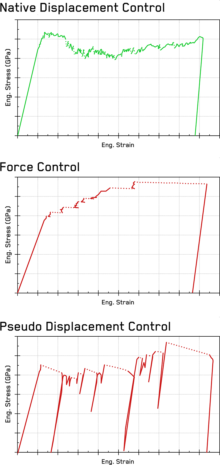 Figure 1. Illustrations of the effect of system control mode on microcompression stress-strain behavior.
In a force-controlled system, intermittent plasticity events manifest as strain bursts. This is commonly attributed to dislocations exiting the pillar free surface. This decrease in dislocation density relieves internal strain and locally lowers the strength of the material, causing a sudden yielding event. In force-control, during this event the indenter system continues to rapidly strain the material at a constant force level until the material generates sufficient new dislocations or otherwise strain hardens sufficiently by some other mechanism to support the level of force. If the sampling rate is sufficiently high, this event can be resolved to show an overshoot in penetration at the end of the strain burst, which dynamically recovers before further loading occurs. This produces local spikes in the applied strain rate during each event, preventing constrain strain rate testing. Also, under force control, the material is not allowed to strain soften, as the force is continually increased by the system, so a strain softening event or a fracture will cause the system to rapidly penetrate further at an apparently constant level of force – smashing the pillar into its substrate.
If a natively force-controlled system is run on a feedback control loop to allow pseudo displacement-control, a different variety of strain burst occurs during intermittent plasticity. The system detects the deviation from its target displacement rate at the speed of its feedback loop and then tries to rapidly reduce the applied force to return to the target displacement rate. However, as the high speed of the strain burst produces a significant positive deviation from the target displacement rate, pseudo displacement-controlled systems typically reduce the force to a degree proportional to the strain burst deviation.
For large bursts, this can result in a complete unloading of the sample [5]. For smaller events, this may produce small load drops like those seen in native displacement control. However, the increase in strain from each burst is still present, changing the observed strain hardening behavior. In pseudo displacement control, the observed sizes of intermittent plasticity events are a complicated function of the time constants of the control loop and the stiffness of the measurement system.
High Temperature Operation
For high temperature testing, several technical features are required to allow testing to be performed in conditions similar to room temperature. Ideally, a system operated at high temperatures should behave identically to how it performs under ambient conditions with a similar degree of ease of use, no changes in dynamics or noise, and stable performance over long test periods. To achieve this, the high temperature module of the FT-NMT-04 was designed with a number of features - Figure 2.

Figure 2. NMT04 with high temperature module features labeled. A variety of clamp geometries are available to accommodate different sample shapes. Cooling copper braids not shown.
To remove any possible vibrations from turbulent fluid flow, cooling of the system is employed purely through passive means using copper braids to conduct the heat away to a large heat sink, which is conductively cooled from the outside of the SEM chamber. This removes any danger of water leaks inside the vacuum chamber, prevents any mechanical vibrations during operation, and provides a constant noise floor, independent of temperature.
However, such conductive cooling is only possible while the heat fluxes are relatively low. To reduce this, the heated components of the system were specifically designed to be as small as possible, to reduce the thermal mass, and were isolated using thermal gaps and insulating components. The system was also designed to have a minimum of extra connections, so that there would be no stray wires to influence the dynamics or positioning capabilities of the system.
The low thermal mass of the heated portion of the indenter tip on the MEMS heater, in particular, is very important to allow fast temperature adjustments. This allows the tip to be rapidly matched with the sample surface temperature using an automated procedure. This consists of performing a series of surface find procedures, where the indenter is rapidly brought into contact with the surface and briefly held there at a constant force. Any deviations in displacement during the hold period are noted and used to align the tip and surface temperature. The tip is then retracted and the procedure repeats until the user is satisfied with the degree of alignment. This procedure automatically accounts for thermal expansion of the system components, as it effectively follows the sample surface through a series of surface finds and retractions.
This combination of precisely-aligned indenter and sample temperatures and stable thermal gradients within the surface frame are essential for achieving low thermal drift (displacement changes due to thermal expansion) during measurements.
In Situ Observation
Performing testing in situ in a scanning electron microscope offers several advantages. The observational capability of the microscope greatly facilitates positioning of the indenter tip over the feature of interest, which is particularly important for FIB-machined micro-geometries such as sub-micron pillars and cantilevers that may be difficult to resolve by optical microscopy. This prevents misalignments from interfering with testing and increases testing speed and reliability dramatically. It also allows precise measurement of sample geometry before, during, and after the test to ensure that dimensions used for stress-strain calculations are accurate.
Testing in the SEM also allows in situ observation of the deformation processes (Figure 4). This is particularly useful as a function of temperature, as deformation mechanisms can change with increasing temperature. This can be combined with a wide variety of analytical detectors within the SEM, such as electron back-scattered diffraction (EBSD) or scanning transmission electron microscopy (STEM), to increase the observational capabilities.
Lastly, the SEM chamber also provides benefits. The SEM’s mechanical vibration isolation reduces any laboratory mechanical noise from being transmitted to the indenter. The vacuum environment of the chamber significantly oxidation at elevated temperatures, which is difficult to achieve with gas environments [3].
Experimental Procedures
Silicon pillars were fabricated by modern lithography patterning combined with reactive ion etching (RIE) [6] on -orientated Si single-crystal wafers. After etching, an additional surface cleaning was performed to remove fluorocarbon residues deposited by the plasma etch on the surface of the pillars. This resulted in 4.5 µm diameter, taper-free pillars with and aspect ratio (diameter/height) of 3. Full details on sample production are available in previous work on these samples [7].
Microcompression testing was performed using an NMT04 In-Situ SEM Nanoindenter with a FT-S200,000-HT sensor fitted with a diamond Berkovich flat punch. Testing was performed in situ in a Zeiss EVO 25 SEM at an acceleration voltage of 10 kV. Displacement rates for each pillar were selected to produce a constant strain rate of 0.004/s. Testing was performed at temperatures of 25, 200, 400, 600, and 800 °C. During each temperature ramp, tip temperature matching was performed using the procedure described earlier. Engineering stress-strain behavior was calculated using the pillar’s height and diameter, and elastic pillar sink-in displacements were corrected using the procedure described in [8].
Results
Engineering stress-strain behavior of the á100ñ-oriented lithography silicon pillars as a function of temperature is shown in Figure 3. The Young’s modulus is seen to closely followed the expected modulus of á100ñ-oriented silicon at ambient temperature (E = 130 GPa). Small non-linearities can be observed in the initial portion of the loading curve due to debris from indenter-sample reactions at elevated temperatures [8]. The typical precision microcompression measurements of elastic modulus is on the order of 5% [9], due to the relatively small fraction of elastic vs. plastic deformation in this geometry. This precision is generally insufficient to characterize Young’s modulus variations, which in silicon varies less than 1% per 100 °C [10].
![Engineering stress-strain behavior of 4.5 µm diameter, [100]-oriented Silicon micropillars tested from ambient temperature to 800°C.](https://www.oxinst.com/learning/uploads/inline-images/ni-an2-fig3-750-20250523125309.png)
Figure 3. Engineering stress-strain behavior of 4.5 µm diameter, [100]-oriented Silicon micropillars tested from ambient temperature to 800°C.
The primary reason for employing the micro-pillar geometry is not to study elasticity but to study plasticity in small volumes. By performing in situ micro-compression tests, both stress-strain behavior and observations of deformation mechanisms can be acquired simultaneously. This highlights the unique capability of the combination of high temperature and in situ testing to visualize transitions in behavior with temperature.
Figure 4 illustrates the transitions in deformation and failure mechanisms of silicon with increasing temperature. At temperatures below 200 °C, pillars were observed to fail by fracture at the base. At 200 °C, a small amount of plasticity was observed prior to failure. At temperatures greater than 200 °C, deformation was observed to primarily occur by dislocation glide on slip system. This transition was also marked by the ‘classic’ shape of the stress-strain curves with the appearance of a lower yield plateau consistent with ‘easy glide’ [11] after dislocation nucleation during the upper yield point. This is particularly noted at the highest temperature of 800 °C. This highlights the native displacement-control of the system.
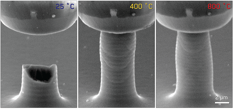
Figure 4. Secondary electron micrographs captured at 10% strain during in situ deformation at various temperatures, illus-trating the brittle to ductile transition from ambient to high temperatures.
Above the transition temperature of ~200 °C, dislocation glide is initially localized on a few slip planes as seen at 400 °C. At higher temperatures, the dislocation motion becomes delocalized onto more slip planes and deformation becomes more homogeneous, as notable in Figure 4.
Discussion
Due to silicon’s importance as a functional and structural material, there have been numerous investigations of its mechanical properties - Figure 5. Due to silicon’s brittleness, literature measurements fall into two different categories: micro-scale [8, 12-15] and macro-scale under confining pressure [11, 16-18]. In general, over the temperature range investigated in this application note, the trend in yield strength vs temperature follows a sigmoidal shape due to transitions in dislocation mechanisms [14]. Macro-scale measurements were performed at lower strain rates (ε̇ = 2 × 10⁻⁵ s−1) to prevent early fracture. Most micro-scale measurements are performed at higher speeds to acquire more statistics on multiple samples. However, Rabier et al. [15] demonstrated that good agreement is seen between micro- and macro-scale measurements at similar strain rates.
Micro-scale measurements in the literature all show close agreement in the lower temperature regimes. The most closely related dataset to the current work is that of Korte et al. [12], who compressed 2 µm diameter silicon pillars. Excellent agreement is observed between these results and the current work at lower temperatures. At higher temperatures, the current results extend the trend with temperature further, revealing over an order of magnitude higher strength in micro- vs. macro-scale samples. This is much greater than previously observed size effects at low temperatures [19]. This is consistent with the increased size effect observed in [14] at elevated temperatures up to 500 °C.
![Yield strength of silicon as a function of temperature comparing to literature values of upper yield from micro-compression [8, 12, 15] and micro-tension [13] and of lower yield values from bulk compression using high hydrostat-ic confining pressure [11, 16-18].](https://www.oxinst.com/learning/uploads/inline-images/ni-an2-fig5-750-20250523125426.png)
Figure 5. Yield strength of silicon as a function of temperature comparing to literature values of upper yield from micro-compression [8, 12, 15] and micro-tension [13] and of lower yield values from bulk compression using high hydrostat-ic confining pressure [11, 16-18].
Conclusion
In this application note, high temperature microcompression was employed to investigate the deformation of lithography silicon micropillars at temperatures up to 800 °C. Stress-strain behavior at high temperatures displayed a characteristic upper yield point followed by a lower yield plateau consistent macro-scale behavior, which was only possible due to the native displacement control of the test system. Elastic behavior was consistent with literature values within the expected precision of the microcompression technique. In situ observation revealed transitions deformation morphology suggestive of dislocation mechanism transitions. Yield behavior observed in this work was consistent with previous micro-scale measurements and extends on their trends in strength and size effects with temperature to 800 °C.
References
- M.D. Uchic, D.M. Dimiduk, J.N. Florando, W.D. Nix, Science, 305 (2004) 986-989.
- J.R. Greer, J.T.M. De Hosson, Progress in Materials Science, 56 (2011) 654-724.
- J. Wheeler, D. Armstrong, W. Heinz, R. Schwaiger, Current Opinion in Solid State and Materials Science, 19 (2015) 354--366.
- J.M. Wheeler, C. Niederberger, C. Tessarek, S. Christiansen, J. Michler, International Journal of Plasticity, 40 (2013) 140-151.
- P. Wang, F. Liu, Y. Cui, Z. Liu, S. Qu, Z. Zhuang, International Journal of Plasticity, 107 (2018) 150-163.
- J.K. Bhardwaj, H. Ashraf, in: Micromachining and Microfabrication, International Society for Optics and Photonics, 1995, pp. 224-233.
- M. Chen, L. Pethö, A.S. Sologubenko, H. Ma, J. Michler, R. Spolenak, J.M. Wheeler, Nature Communications, 11 (2020) 2681.
- J.M. Wheeler, J. Michler, Review of Scientific Instruments, 84 (2013) 045103.
- I.-S. Choi, Y. Gan, D. Kaufmann, O. Kraft, R. Schwaiger, Journal of Materials Research, (2012).
- N. Ono, K. Kitamura, K. Nakajima, Y. Shimanuki, Japanese Journal of Applied Physics, 39 (2000) 368-371.
- J. Rabier, P.O. Renault, D. Eyidi, J.L. Demenet, J. Chen, H. Couvy, L. Wang, Physica Status Solidi (C) Current Topics in Solid State Physics, 4 (2007) 3110-3114.
- S. Korte, J.S. Barnard, R.J. Stearn, W.J. Clegg, International Journal of Plasticity, 27 (2011) 1853-1866.
- S. Nakao, T. Ando, M. Shikida, K. Sato, Journal of Micromechanics and Microengineering, 16 (2006) 715-720.
- M. Chen, J. Wehrs, A.S. Sologubenko, J. Rabier, J. Michler, J.M. Wheeler, Materials & Design, 189 (2020) 108506.
- J. Rabier, A. Montagne, J.M. Wheeler, J.L. Demenet, J. Michler, R. Ghisleni, physica status solidi c, 10 (2013) 11-15.
- J. Castaing, P. Veyssiere, L.P. Kubin, J. Rabier, Philosophical Magazine A: Physics of Condensed Matter, Structure, Defects and Mechanical Properties, 44 (1981) 1407-1413.
- J.L. Demenet, in, University of Poitiers, France, 1987.
- J.L. Demenet, J.C. Desoyer, J. Rabier, P. Veyssiere, Scripta Metallurgica, 18 (1984) 41-45.
- B. Moser, K. Wasmer, L. Barbieri, J. Michler, Journal of Materials Research, 22 (2007) 1004-1011.

