Introduction
It is becoming increasingly important to be able to characterise materials on the nanoscale. Despite significant technological developments in recent years, the EBSD technique is still limited by the pattern source volume to resolutions in the order of 25–100nm; this is insufficient to measure accurately truly nanostructured materials (with mean grain sizes below 100nm). A new approach to SEM-based diffraction has emerged, namely using an electron transparent sample coupled with conventional EBSD hardware and software. This technique, referred to as transmission EBSD (t-EBSD: Keller and Geiss, 2012) or SEM transmission Kikuchi diffraction (TKD: Trimby, 2012) has been proven to enable spatial resolutions better than 10nm, and is ideal for routine EBSD characterisation of both nanostructured and highly deformed samples.
This application note describes the set up required for working with an EBSD system in transmission mode, using a NordlysNano EBSD detector and AZtecHKL. It illustrates the application of TKD to a nanostructured nickel sample and a highly deformed stainless steel, both of which were impossible to characterise using conventional EBSD.
Method
Samples for TKD are prepared in a standard way as for transmission electron microscopy. Typical techniques involve electropolishing, ion beam thinning or using a focused ion beam SEM. The sample thickness is critical: best results are achieved using relatively thin samples, in the range of 50nm to 150nm.
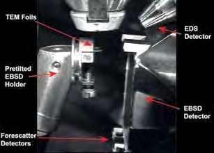
The samples are mounted to be horizontal in the SEM chamber, at a level above the top of the EBSD detector's phosphor screen. This is typically at a short working distance (e.g. 5–10mm), depending on the position of the EBSD detector. In this example, the sample was mounted using a pretilted holder and a small microclamp: the SEM stage was tilted to 20°, ensuring that the samples (TEM foils) were horizontal and that the SEM stage was not under the transmitted electron beam, as shown in the image below.
Here a NordlysNano EBSD detector coupled with AZtec software was used for data acquisition. The NordlysNano detector has the highest sensitivity and is therefore the best detector for this application. An example TKD pattern is shown below, taken from a deformed Ni-Cu alloy.
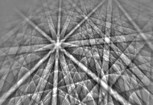
The electron beam is focused onto the electron transparent sample and the diffraction pattern is projected from the lower surface onto the phosphor screen. The majority of the pattern signal originates from the lowermost part of the sample, allowing successful analyses of samples in which the grain size is smaller than the sample thickness. Typically the maximum acceleration voltage of the SEM is used (normally 30kV), with a large beam current (i.e. 1nA to 20nA) and with the beam optimised to give the best depth of field. Orientation mapping is carried out in the same way as for conventional EBSD, although no tilt correction or dynamic focus is required, and step sizes can be as small as 2nm.
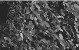
Forescatter detectors, positioned below the Nordlys phosphor screen, can also be used to give orientation contrast images of electron transparent samples. The example image shows an equal channel angular pressed (ECAP) Aluminium alloy. Grain structure is clearly visible and the field of view is 30μm across.
Results
Nanostructured Example: Nickel
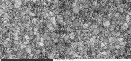
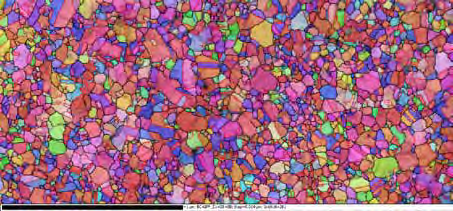
An electrodeposited nanocrystalline nickel sample was prepared for analysis using an ion beam thinner and then mounted for TKD analysis. The sample had a mean grain size of under 50nm, and previous attempts to analyse similar samples using conventional EBSD were only able to measure the largest of the grains (e.g. Klement et al., 2007). The TKD orientation map shown here was collected using a step size of 4nm and with an indexing rate over 80%.
The pattern quality map (band contrast) illustrates how clearly even the smallest grains have been resolved, and the cleaned inverse pole figure map shows the details of the grain structure, including the prevalence of sigma 3 CSL boundaries (shown in red). The scale bars in both images mark 1μm.
Highly Deformed Example: Stainless Steel
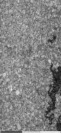
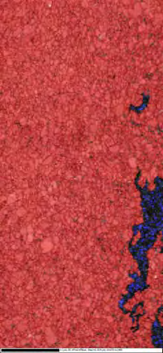
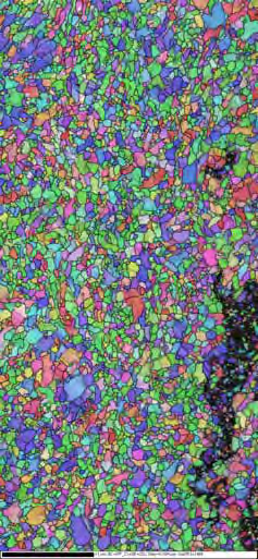
The high dislocation densities in heavily deformed materials make them very difficult to analyse using conventional EBSD. The superior resolution of TKD enables effective characterisation of even the most highly deformed samples. In this example a duplex stainless steel sample has been deformed at room temperature by high pressure torsion, resulting in significant grain size refinement and intragranular deformation. The ferrite (BCC) phase develops a final grain size below 100nm, whereas the austenite (FCC) is even finer grained, with high resolution TEM imaging indicating a mean grain size below 10nm. TKD mapping with a step size of 4nm was used to characterise the sample, with the results shown below. The pattern quality map (left image) shows clearly the fine grain size, with a few areas with significantly poorer quality patterns. The phase map (centre image) shows that the poorer patterns are from areas of the FCC phase, in which the TKD technique can only resolve the larger grains. The cleaned orientation map (right) illustrates the lack of texture in this sample, but also the deformation within the larger grains (> 100nm) exhibited by substantial intra-grain orientation variations. The scale bars mark 1μm.
Summary
These results illustrate how, with the AZtecHKL EBSD system, it is possible to characterise truly nanocrystalline materials using the newly developed TKD technique. The TKD spatial resolution is in the order of 5–10nm, which also enables effective measurement of highly deformed materials that would be extremely challenging using conventional EBSD. The results are comparable to those achieved using automated diffraction techniques in the TEM, but with all the additional benefits and flexibility offered by an SEM. In addition, all the post-processing tools developed for standard EBSD are applicable to TKD datasets.
Acknowledgements
Uta Klement, Yang Cao and Katja Eder are thanked for providing the samples. Adam Sikorski is thanked for helping with sample preparation. All analyses were carried out at the Australian Centre for Microscopy & Microanalysis at the University of Sydney. Pat Trimby is thanked for providing the data and writing the application note.
References
- R.R. Keller and R.H. Geiss, J. Microscopy 245 (2012), 245–251
- P.W. Trimby, Ultramicroscopy 120 (2012), 16–24
- U. Klement and M. da Silva, Journal of Alloys and Compounds 434–435 (2007) 714–717

