Introduction
The current demands from optical interconnect, LIDAR technology or face recognition is driving the VCSEL industry to grow faster. VCSEL manufacturing is rapidly scaling up across the world and the VCSEL fabrication process has to achieve ever higher yield and quality. Applications, such as 3D sensing, focus on maximum power conversion with arrays of VCSELs for higher combined output power. Within an array, the threshold current and differential quantum efficiency have to be uniform from laser to laser. This requires very good control of epitaxy but also very good control of the shape of the mesa. As the need for denser array increases, challenges on uniformity, line width and aspect ratio emerge.
With a strong process expertise and extensive device understanding, Oxford Instruments Plasma Technology has developed advanced plasma processing solutions to deliver the device performance and yield demanded by the VCSEL market. In this white paper, we focus on how to best control the geometry of the mesa for wafer size up to 150 mm. We review the key requirements for achieving either a tapered or vertical profile with precise control of the depth of the mesa.
Main Fabrication Steps of VCSEL Structures
The simplicity of the VCSEL structure allows for high volume manufacturing at very efficient cost. Compared to edge emitting lasers, more VCSELs can be manufactured per wafer and on larger wafer sizes. The vertical fabrication of VCSELs also allows for a high level of integration of additional components. Photo detectors, mirrors, circuitry and other components can easily be integrated onto the structure to achieve chip on board (COB) technology. As the technology evolves, multiple designs have been developed for specific applications. Here we take a look at a simplified process flow to design the laser cavity.
Multiple processing steps are required to fabricate VCSELs. The table in Figure 1 below gives a simplified breakdown of each step of fabrication of GaAs based VCSEL, highlighting the Oxford Instrument solution for relevant steps. The Cobra ICP system delivers uniform process on wafers up to 200 mm. The VCSEL market is currently moving towards 150 mm so most of the work demonstrated here is focused on 100 mm to 150 mm wafer size.

Fig. 1 — Simplified process flow for fabricating VCSEL cavity (top) and Cobra module (bottom)
Mask Matters
The profile of the mask influences the profile of the mesa. The mesa etch is an anisotropic etching process with the etch angle having some dependence on the selectivity and original mask profile. A very sloped mesa profile will require a very sloped mask. In this case, a photo resist mask can be used to achieve shallower angle.
Depending on the target profile of the mesa, a photo resist mask or a hard mask can be used. Hard masks developed for mesa etching are usually made of SiN or SiO2. When using a hard mask, a denser film will give higher selectivity to the DBR stack and allow deeper etching depth. A hard mask is an option when the mask opening process has been sufficiently optimised to demonstrate the target profile. However, careful process design must be applied when slopping the mask as using passivation can lead to excess roughness on the sidewalls. When the mask is used to control the mesa profile, control of selectivity would also allow control over the profile of the mesa. Using the Cobra ICP system, Oxford Instruments Plasma Technology has demonstrated mask profile from 60° to 90°.
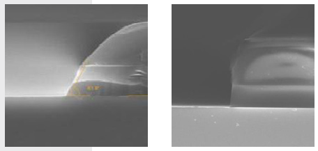
Fig. 2 — SiN Mesa mask profile angle (a) 60° (b) 90°
Precise and Uniform Mesa Height and Profile
A series of parameters can be assessed after etching to verify the geometry of the mesa. Some of the key parameters measured are the top and the bottom diameter of the mesa. These parameters are often measured along with the profile angle. A precise control of the mesa height across wafer and from wafer to wafer is also necessary.
The DBR structure is made of GaAs/AlGaAs pairs with varying content of Al. The layer stack is commonly dry etched using ICP mode. ICP etching has the benefit of operating at very low pressure yet high plasma density. Processing at low pressure favours highly directional etching in a regime with high mean free paths. This allows achievement of high anisotropy with an easier control of the critical dimension. The process is also run using electrostatic clamping as this provides minimum edge exclusion and is commonly used in production environment.
The chemistry used is chlorine-based. Chlorine is reactive with Gallium, Arsenide as well as Aluminium and forms volatile by-products at processing temperatures. The boiling point of the by-products is given in the table in Figure 3.
| III-V element | By-products | Boiling point (at Vapour pressure Torr) |
| Ga | GaCl3 | 50°C (at 2) |
| As | AsCl3 | 100°C (at 1) |
Fig. 3 — Boiling point of by-products. Courtesy of Indium Phosphide and related materials by Avishay Katz
Designing a process to obtain a mesa with the desired profile relies on a good control of the concentration of various ions species and radicals. This is mainly determined by the gas flow, the ICP power and the pressure. The profile is then a result of a balance between passivation and etching.
The low bond energy of GaAs means that the process is mainly chemical and does not require high ions energy. This can be beneficial in achieving high etching rates; however, the process also tends to etch slower in the centre. To maximise the yield, uniform etching rate relies on maintaining the same availability of species across wafer. This can be achieved either by minimising residence time or adjust to have uniform loading everywhere.
The process being chemical also causes the profile to show a foot. As the etching rate tends to be faster at the centre of open area, a difference in etching depth appears from the centre of the trench to the edge. This difference is commonly quantified as a percentage of the full etching depth. An example of a foot is given in Figure 4 below. If not well controlled, the foot can act as an error on the depth accuracy and be detrimental to the laser behaviour. Moreover, the etching should ideally stop within one layer of the DBR which becomes impossible if the foot is larger than the thickness of one DBR layer.
Fabricating a sloped mesa with low footing is generally easier than fabricating a vertical mesa with low footing. When etching a sloped mesa, the ions tend to glance off the sidewalls before hitting the bottom etched surface. This causes the etching rate to slow at the centre of the trench. The foot and the profile are both controlled by balancing passivation and etching. High passivation will favour a sloped profile and low footing.
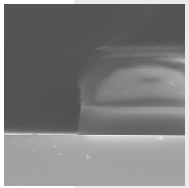
Fig. 4 — VCSEL mesa etch cross section with significant footing (13%)
To provide fine control of the etching depth, the etching depth is also actively monitored using optical emission spectroscopy (OES). It is possible to track the oscillation in the concentration of Gallium and Aluminium as we etched through the various layers of the DBR, because of the excellent uniformity and low footing achieved on the Cobra ICP system. This method is best suited to fully automated line production. An example of OES trace is given in Figure 5. This OES trace was captured on the Cobra ICP system for a sloped mesa profile with a uniformity of the etching depth across wafer within ±1%. As seen on the trace, each oscillation is clearly defined. Each oscillation corresponds to a pair of the DBR structure and the process can be set to stop on any of these peaks by tracking the first derivative of the signal.
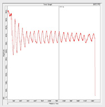
Fig. 5 — OES trace of Gallium line for a sloped mesa. Within wafer uniformity ±1%.
An alternative to OES monitoring is laser reflectometry. This method also provides in situ real time monitoring by tracking the reflectance of a laser beam directed at the surface of the wafer. It provides information on a single point and require reliable wafer placement. An example of laser signal trace is given in Figure 6.
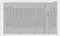
Fig. 6 — Reflectivity as a function of etching time
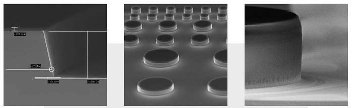
With process recipes developed at Plasma Technology, an excellent combination of good profile control and low footing has been achieved using the Cobra ICP system and monitoring of etching depth. Results achieved on 100 mm and 150 mm wafers are shown in the SEM below. As shown in the SEM, the profile and footing are very uniform across 100 mm wafers. The surface and sidewalls are also very smooth. Devices produced using this recipe also passed the accelerated lifetime testing.
Conclusions
Oxford Instruments Plasma Technology has a long history of working closely with the Compound Semiconductor community to deliver the maximum device performance and manufacturing efficiency. We have developed advanced plasma processing solutions to deliver the device performance and yield demanded by the VCSEL market.
We have demonstrated high precision manufacturing of VCSEL mesas from masking to etching of the mesa, and devices passing accelerated lifetime testing. We have achieved conventional vertical profile as well as sloped profile required in 3D sensing. Both masking and mesa etching are demonstrated at excellent uniformity over up to 150 mm wafer size, which is critical for uniform threshold current and differential quantum efficiency in VCSEL arrays. Plasma Technology patented ESC associated to key understanding of plasma chemistry have allowed us to repeatedly produce mesa with uniform profile and extremely low footing. Additionally, we have used our experience in designing solutions to monitor plasma processes to demonstrate fully automated endpoint detection and therefore fine control of end layer, i.e mesa height.

