The Raman Principle
The Raman effect is based on the inelastic scattering of light by the molecules of gaseous, liquid or solid materials. The interaction of a molecule with photons causes vibrations of its chemical bonds, leading to specific energy shifts in the scattered light. Thus, any given chemical compound produces a particular Raman spectrum when excited and can be easily identified by this individual "fingerprint."
Raman spectroscopy is a well-established, label-free and non-destructive method for analyzing the molecular composition of a sample.
Raman Imaging
In Raman imaging, a confocal microscope is combined with a spectrometer and a Raman spectrum is recorded at every image pixel. The resulting Raman image visualizes the distribution of the sample's compounds. Due to the high confocality of WITec Raman systems, volume scans and 3D images can also be generated.
No Need for Compromises
The Raman effect is extremely weak, so every Raman photon is important for imaging. Therefore WITec Raman imaging systems combine an exceptionally sensitive confocal microscope with an ultra-high throughput spectrometer (UHTS). Precise adjustment of all optical and mechanical elements guarantees the highest resolution, outstanding speed and extraordinary sensitivity – simultaneously!
This optimization allows the detection of Raman signals of even weak Raman scatterers and extremely low material concentrations or volumes with the lowest excitation energy levels. This is an unrivaled advantage of WITec systems.
Sensitivity: A high confocality increases the signal-to-noise ratio by reducing the background. With the UHTS Series, WITec developed lens-based, wavelength-optimized spectrometers with a spectral resolution down to 0.1 cm-1 relative wavenumbers.
Resolution: Lateral resolution is physically limited to ~200 nm, depending on the wavelength of the incident light.
Speed: The more sensitive a system is, the shorter the acquisition time for a single spectrum. WITec's Ultrafast Raman Imaging reduces acquisition times for single Raman spectra down to well below 1 ms.
Introduction
Structured substrates are widely employed in semiconductor research and especially in current semiconductor development. Demanding requirements in device quality and reliability make it increasingly important to have a detailed knowledge of the inherent strain and crystalline properties of device structures. X-ray diffraction is commonly used in order to probe film thicknesses, lattice constants and strain states of layer structures and scanning electron microscopy (SEM) is used to inspect surfaces and defects in the structure to understand the growth history. In this application note results are presented of 3D confocal Raman imaging measurements that reveal changes in the signal which can be attributed to strain as well as to changes in the lattice structure.
Sample Description
The sample used was an unintentionally doped GaN layer of 20 μm thickness grown by metal organic vapor phase epitaxy (MOVPE) and subsequent overgrowth by hydride vapor phase epitaxy (HVPE) on a c-plane patterned sapphire substrate (PSS). Fabrication of the pattern and growth was performed at the Ferdinand-Braun Institute in Berlin. The sapphire substrate was patterned with I-line beam stepper lithography using a KMPR 1000 negative photoresist and ion coupled plasma (ICP) etching. The investigated honeycomb-like structure has a trough depth of 4.5 μm with a ridge width of 3.5 μm and a pitch of 12 μm.
This and similar patterns are relevant for light emitting devices as they allow for epitaxial lateral overgrowth (ELO) to reduce threading dislocation density and improve the internal quantum efficiency or serve for embedded periodic deflectors to enhance light extraction [1].
Figure 1 depicts a cross-sectional SEM micrograph of the sample. It consists of the patterned sapphire with troughs and ridges at the bottom followed by GaN grown in the troughs and in part of the ridge edges. Finally a coalesced GaN layer covers the pattern with slight contrast above the trough and ridge regions. Vertical lines are cleaving steps which are denser in the GaN directly grown on the sapphire surface in the troughs or on top of the ridges.
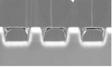
Fig. 1 — SEM image of a GaN layer grown on a sapphire substrate. Vertical lines are steps due to cleavage with a higher line density in regions of direct contact between GaN and sapphire.
Figure 2 shows SEM images of the pattern after the ICP process (A), after the growth of the first 3 μm thick GaN film on the PSS substrate by MOVPE (B), and after the growth of another 17 μm thick GaN layer by HVPE (C).
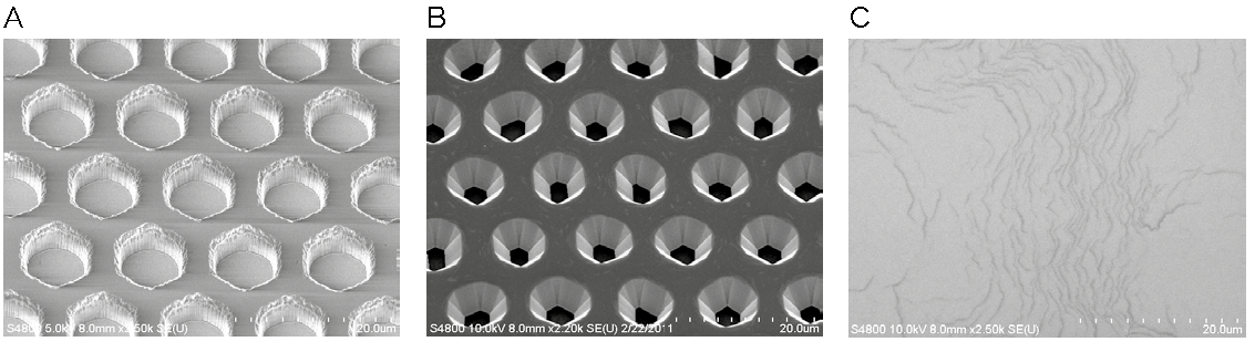
Fig. 2 — SEM images of different states of GaN growth. (A) After the etching process. (B) After the growth of the first 3 μm GaN film. (C) After the growth of the additional 17 μm thick GaN layer.
Experimental Section
The samples were examined using an alpha300 confocal Raman microscope with a frequency-doubled Nd:YAG laser for excitation (λ=532 nm). The light was coupled into the microscope using a photonic fiber and brought onto the sample using a dichroic mirror and a 100x NA 0.9 air objective. In the detection beam path, the Rayleigh-scattered light was filtered out using an edge filter and a 50 μm core-diameter fiber was used as a confocal pinhole, providing good depth resolution while maintaining excellent collection efficiency. The light was then directed to a UHTS300 spectrometer equipped with an 1800 g/mm grating (BLZ 500 nm) and an EMCCD camera. The XY positioning of the sample was achieved using a piezoelectric scanning stage and a stepper motor was used for focus control (10 nm per single step).
The Raman spectra were recorded as a depth-scan along an interesting axis along the sample (240 x 80 points on a scan area of 60 x 20 μm2) as shown in Figure 3. 3D stack scans were additionally performed and analyzed (180 x 45 x 20 points with a scan volume of 60 x 15 x 20 μm3).
For each of the scans a spectrum was recorded at every pixel with an integration time of 20 ms/spectrum. Using the WITec Suite software, the relevant information was extracted and displayed as color-coded Raman images. The results enabled the generation of a 3D image of the Raman features throughout the investigated sample volume.
Results
Figure 3A shows the white-light image of the sample acquired using the built-in ocular video camera and the stitching function of the system. The image consists of 100 individual images and allows for a larger overview with high-resolution. The red square in the image indicates the area from which the single high-resolution white-light image using the 100x objective was taken (Figure 3B). In this image the holes in the structure appear in different colors due to differences in the white light interference, which depends on the distance between the upper surface of the GaN grown in the holes and the lower GaN surface of the coalesced layer. The green area in Figure 3B shows the area at which the XY scan and the stack scan was performed and the red line indicates the plane in which the single depth-scan was performed.
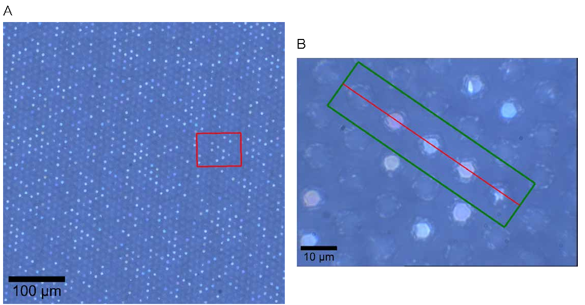
Fig. 3 — Video images of GaN grown on a sapphire substrate. (A) Large area image. The stitched image was acquired using a 100x objective. The red square shows the position of the high-resolution video image shown in (B). (B) High-resolution image of the area of interest. The area for the Raman stack scans is shown in green and the red line indicates the position of the single depth-scan.
Analysis of Spectral Features in the Sample
Using a depth-scan, three areas could be detected in the sample. Figure 4A shows the false-color Raman image with the spectra in corresponding colors shown in Figure 4B. In the red areas, the spectrum shows the typical features of GaN spectra [2]. In the green areas, which coincide with the edges of the ridges, an enhanced fluorescence can be seen. This fluorescence is located primarily in the low-wavenumber range of the spectrum (see green spectrum in Figure 4B). The blue areas are located directly above the holes and can be spectrally characterized by a strong reduction of the intensity of the peak near 735 cm-1 relative wavenumbers and a broad peak on the higher wavenumber side of this peak. This is shown in the zoomed view of the relevant spectral detail (Figure 4B). This peak shift and broadening may hint at a material of lower crystalline quality. The inclusion of contaminations in non-c-planar growth at these positions could give rise to the coupled non-planar optical phonons A1(LO)+ or A1(L)+.
Figure 4C shows one layer extracted from the stack scan in which the typical spectral features discussed in the last paragraph are again displayed using the same color code. The fluorescence (green areas) is located at the walls of the ridges and the areas of lower intensity of the 735 cm-1 peak (shown in blue) are located on the interiors of the holes.
The layers recorded in the image stack were evaluated in a manner similar to the layer shown in Figure 4C and combined into a 3D reconstruction using the ImageJ software. Figure 4D shows a 3D view of the reconstructed 3D structure. As before in Figure 4C, the location of the fluorescence and the regions of a weaker 735 cm-1 peak can be clearly identified at the positions of the holes.
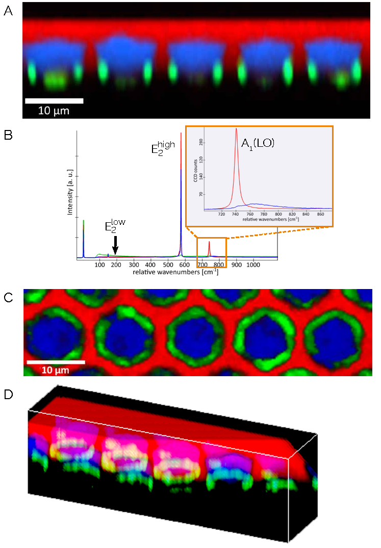
Fig. 4 — Raman imaging of GaN grown on a sapphire substrate. All Raman images are color-coded according to the spectra in (B). (A) Depth scan Raman image performed along the red line shown in Figure 3B. The holes in the structure were located precisely underneath the blue-colored areas. (B) Corresponding Raman spectra. (C) Color-coded Raman image of a single plane of the area marked in green in Figure 3B. (D) 3D Raman volumetric representation of the same region, consisting of scans performed at different focal planes (180 x 45 x 20 pixels, 60 x 15 x 20 μm3).
Peak-Shift Analysis
It has been shown by various authors [3-5] that strain in crystalline samples can be correlated with Raman peak shift. Using the measurements presented above, a peak-shift analysis of the spectra was performed. For this purpose the peak near 570 cm-1 relative wavenumbers of each spectrum in each of the scans was fitted using a Lorentzian curve. This results in a very accurate determination of the position of the Raman peaks with a typical uncertainty of 0.02 cm-1 relative wavenumbers.
Figure 5A shows the position of this peak for the depth-scan. There are various areas in which the Raman line is shifted to lower wavenumbers (green) as well as various areas where it is shifted to higher wavenumbers (red). Two representative spectra illustrating these peak shifts are shown in Figure 5B. Here, experimental data recorded by the CCD camera as well as the Lorentzian fitting curve are shown. Figure 5C shows the distribution within the sample in one of the planes extracted from the stack scan. Again various domains can be seen. However, these discrete images in single planes make it quite difficult to draw a clear picture of the peak shift and the resulting strain distribution in the sample. Using the complete information collected by the stack scan and performing a 3D reconstruction permits a much clearer analysis.
Figure 5D shows this 3D distribution with shifts to lower wavenumbers again marked in green and shifts to higher wavenumbers shown in red. The image underneath is the intensity of the peak near 735 cm-1 relative wavenumbers of a plane just above the holes and allows for the spatial association of the stress fields with the position of the holes. It is readily apparent that the stress fields propagate from the interface to the surface mainly in tube-like structures, which was not obvious in the 2D views of the sample.
The overall differences in the position of the peak are quite small (< 1 cm-1) and thus the overall differences in the strain of the GaN are also small. The Raman stress factor for the E2high phonon mode, however, is quite high with –3.4 ± 0.3 cm-1/GPa [6]. Minute changes in the lattice constant can be measured due to the high Raman stress factor making the peak shift visible within highly sensitive Raman spectroscopy [7]. Surprisingly, the compressive strain in this GaN sample is very homogeneous independent of the region (hole or ridge) with the exception of a small, less compressively strained border at the ridge edges where some disturbed GaN growth at the edge walls was observed. Therefore, Raman microscopy has been shown to be an extremely sensitive and useful tool for growth optimization on patterned sapphire substrates.
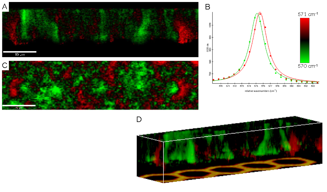
Fig. 5 — Raman peak shifts in GaN grown on a sapphire substrate. (A) Raman peak-shift image of a depth-scan. (B) Color-coded data points and fitted curves of Raman spectra at different positions of the E2high Raman peak near 570 cm-1. (C) Raman peak-shift image of a single layer of the GaN stack scan in (D). (D) 3D representation of the stress fields in the GaN layer. The image in the bottom plane indicates the positions of the pits.
Conclusion
3D confocal Raman imaging was used to probe the properties of GaN layers grown on patterned sapphire substrates. It was shown that an enhanced fluorescence signal can be detected along the perimeter of the etched structures and that the material above this region shows a clearly modified Raman spectrum.
A stress analysis using the exact position of the Raman E2high phonon mode peaks showed tube-like structures where the Raman peaks were down-shifted (less compressive), which propagate from the GaN-sapphire interface up to the surface of the GaN layer. This structure is in good agreement with partially distorted and unintended growth at the edge walls of the ridges observed in the SEM image. While SEM allows for the examination of physical surfaces, Raman has the advantage of being non-destructive and providing very detailed insight into the variations of the strain in group III nitride structures grown on patterned sapphire substrates. The two techniques therefore complement each other ideally.
Acknowledgements
Oxford Instruments WITec would like to thank Dr. Eberhard Richter from the Materials Technology Department of the Ferdinand Braun Institute, Berlin, Germany (www.fbh-berlin.de) for providing the sample along with the invaluable scientific discussion leading to this application note.
References
- M. Cooke, (2011). Technology focus: Nitride substrates. Semiconductor Today, Compounds & Advanced Silicon
- Vol. 6 (7) Sept./Oct. p. 120.
- Kuball, M. (2001). Raman spectroscopy of GaN, AlGaN and AlN for process and growth monitoring/control. Surface and Interface Analysis: An International Journal devoted to the development and application of techniques for the analysis of surfaces, interfaces and thin films
- , 31(10), 987-999.
- Gundel, P., Schubert, M. C., & Warta, W. (2010). Simultaneous stress and defect luminescence study on silicon. physica status solidi (a)
- , 207(2), 436-441.
- Gigler, A. M., Huber, A. J., Bauer, M., Ziegler, A., Hillenbrand, R., & Stark, R. W. (2009). Nanoscale residual stress-field mapping around nanoindents in SiC by IR s-SNOM and confocal Raman microscopy. Optics Express
- , 17(25), 22351-22357.
- Wermelinger, T., Borgia, C., Solenthaler, C., & Spolenak, R. (2007). 3-D Raman spectroscopy measurements of the symmetry of residual stress fields in plastically deformed sapphire crystals. Acta Materialia
- , 55(14), 4657-4665.
- Ahmad, I., Holtz, M., Faleev, N. N., & Temkin, H. (2004). Dependence of the stress-temperature coefficient on dislocation density in epitaxial GaN grown on α-Al2O3 and 6H-SiC substrates. Journal of applied physics
- , 95(4), 1692-1697.
- Gorczyca, I., Christensen, N. E., y Blancá, E. P., & Rodriguez, C. O. (1995). Optical phonon modes in GaN and AlN. Physical Review B
- , 51(17), 11936.

