Front End Plasma Solutions for InP-based Lasers and Photodiodes
Continuously increasing global data traffic is putting pressure on the optical communication network and driving demand for transceivers with more and more bandwidth. InP-based photonic integrated circuits are already firmly established in this market and manufacturing capability is expected to scale up to support the required network infrastructure transformation.
The key applications of InP-based components include lasers for silicon photonics, transceivers in data centres, mobile backhaul, access networks and metro markets. The properties of InP and related compound semiconductor materials make them desirable semiconductors for the manufacture of optoelectronic devices that can operate at high frequencies. Furthermore, their natural wavelength range of operation of 1300 – 1650 nm perfectly matches the optimal spectral range of optical fibres used for fibre optic communications.
Oxford Instruments Plasma Technology has developed advanced InP plasma processing solutions to deliver cost-effective, high-yield and high-performance processing strategies, to support the scaling up of manufacturing capability. In this white paper, we discuss some critical plasma processing steps to produce lasers and photodiodes and share our processing capability.
Main Fabrication Steps of InP-based Lasers and Photodiodes
InP-based lasers and photodiodes are deployed in high volume in today's optical transceivers. For example, distributed-feedback lasers (DFB) have narrow linewidth and high spectral purity, and are widely used in transmitters as a directly modulated laser (DML). The combined demand for 400 Gbps transceivers in intra-datacentres, and for 25 Gbps transceivers in 5G fronthaul antenna, is rapidly driving demand for electro-absorption modulated laser (EML) – devices that transmit at higher bit rates with much lower chirp. As seen in Figure 1, in EML an electro-absorption modulator (EAM) is monolithically integrated in front of the DFB laser to achieve ultra-high-speed modulation. For receivers, InGaAs/InP photodiodes are widely used due to the superior speed, responsivity, and low noise characteristics.

Fig. 1 — Schematic figures of DFB laser and EML. L Source: Oclaro. R Source: Lumentum.
Multiple processing steps are required to fabricate InP-based DFB, EML and photodiodes. Figure 2 gives a simplified breakdown of fabrication steps of InP DFB and EML devices. For photodiodes, the grating etch, regrowth, and facet are not needed. All the material layers that form the basis of an InP laser and photodiodes are laid down using epitaxial growth techniques, while the deposition, masking and etch steps used to incorporate the necessary gratings and waveguides are implemented using plasma processing methods. An array of plasma processing techniques are required to achieve cost-effective and high yield industrial manufacture.

Fig. 2 — DFB and EML fabrication process.
Grating as the Mirrors
The active region of the DFB laser contains a periodically structured element, which builds a one-dimensional diffraction grating providing optical feedback within the laser. The depth and geometry of the gratings need to be precisely controlled in the fabrication process to achieve the desired coupling coefficient and ensure high side-mode suppression ratio (SMSR) and low threshold.
Due to the requirements mentioned above, a dry etch process based on CH4/H2 is an ideal solution for the InP DFB grating etch. Using Oxford Instruments Plasma Technology's Cobra® etch module, we have a process with a moderate etch rate (10 – 40 nm/min) to produce a precise, shallow, time controlled etch (depth typically in the order of 100 nm). The dimensions of the gratings are accurately transferred from the mask because the process exhibits high selectivity. Considering the frequent use of photoresist masks to pattern the gratings, the process utilises an ambient temperature rather than hot process, to avoid photoresist burning. The mask is then stripped post-etch to reveal the high precision gratings. Figure 3 shows a grating etched to a depth of 100 nm at an etch rate of 20 nm/min.
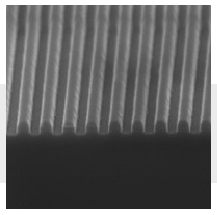
Fig. 3 — InP grating etched to a depth of 100 nm at an etch rate of 20 nm/min.
Ridge Waveguide and Mesa with Vertical Profile and Smooth Sidewall
To produce InP lasers and photodetectors, while each fabrication step is important, the InP Mesa/Ridge etch is arguably the most critical as the properties of the resulting waveguide have a defining impact on the quality of the finished devices. For DFB lasers and the modulator in EMLs, the vertical profile of the ridge waveguide is important for light confinement and mode properties. For photodiodes, the mesa profile can be vertical or tapered to maximise the amount of light that reaches the active layers. For all devices, smooth sidewalls and surfaces are essential since roughness is associated with light scattering and absorption, which reduces amplification relative to loss and consequently diminishes the power of the laser. In addition, smooth surfaces minimise contact resistance throughout the device, thereby maximising the conversion of power to light.
To support manufacturing scale up, a high rate and clean fabrication process is desired to etch ridge waveguides and mesas. Therefore, CH4 should be excluded from the chemistry to avoid polymer contamination. Oxford Instruments Plasma Technology provides world-leading solutions based on chlorine/argon chemistries, which deliver high rate, vertical etch profiles, and smooth etch surfaces. Also, this process is polymer free so the chamber remains clean, for high repeatability. Due to the high reactivity of chlorine with InP and the low volatility of the etch by-product InClx, it is critical to optimally control gas composition, pressure, and plasma powers to balance the etch and passivation components. Oxford Instruments Plasma Technology's extensive experience of working with InP manufacturers ensures the most optimised processes for any device design.
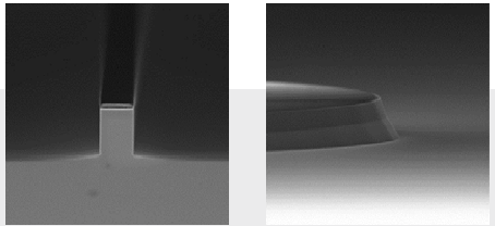
Accurate wafer temperature control is paramount for this process since it determines the evaporation rate of InClx. The low volatility of InClx permits highly anisotropic etching to achieve a deep, vertical, or sloped profile, but if volatility becomes too low, undesired deposition occurs on the developing surfaces which increases roughness. On the other hand, aggressive evaporation rates are associated with undercutting of the mask, therefore process temperatures tend to be greater than 190°C, but not excessive, as this will lead to undercutting. Oxford Instruments Plasma Technology delivers precise control of temperature up to 250°C with uniform temperature distribution across the wafer. Oxford is working at the forefront of InP processing to help industrial manufacturers to maximise their yield. Figure 4 shows InP waveguide and mesa etching for lasers and photodetectors. As seen from the SEM, the profile is well controlled, and the surface and sidewalls are also very smooth.
Mask Matters
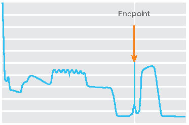
An important aspect of etch control is endpoint detection (EPD). Optical emission spectroscopy (OES) is a fully automated EPD technique which has proven applications and can be used to analyse the composition of the plasma to monitor progress. An example of OES trace is given in Figure 5. This OES trace was captured on the Cobra®, etching a vertical ridge waveguide, with an etch depth uniformity of <±3% across the 3-inch wafer. As seen on the trace, each layer is clearly defined, and the process can be set to stop within any layer (even as thin as ~10 nm). When integrated with processing software, such analysis helps manufacturers to achieve maximum throughput and highly consistent product quality.
In general, a vertical profile waveguide will require a vertical mask, and sloped profile waveguides will require a sloped mask. Roughness on the sidewall of the mask will be transferred directly onto the InP during etch, so an accurate and clean mask is essential to create the desired profile and smooth sidewall in the final InP structures.
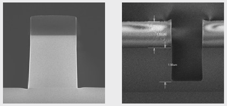
Considering the high run temperatures of the chlorine/argon process, a hard mask such as SiNx or SiOx is preferred since photoresist tends to burn at higher temperatures, causing issues with roughness and mask removal. For hard mask, denser films enable a more selective etch and support a deeper InP etch with a more controllable profile. Additionally, the mask opening process must be sufficiently optimised to demonstrate the target profile without adding excess roughness on the sidewalls. Using the Cobra®, Oxford Instruments Plasma Technology has demonstrated mask profile from 60 to 90° with smooth sidewall and surface, as shown in Figure 6, using high density Plasma Enhanced Chemical Vapour Deposition (PECVD) masking layer.
Passivation Deposition
For InP lasers and photodiodes, the deposition of a passivation layer and further etching to enable electrical contacts to be formed is required. SiNx or SiOx are the materials of choice for the passivation layer and a high film quality is required to demonstrate efficient electrical properties. For dielectric masks, the film density is associated with high selectivity during the subsequent etch. While for passivation, it is directly associated with the insulation of the device, with higher density films resisting the ingress of water more effectively and enables the application of higher voltages prior to breakdown. For photodetector, high density passivation layers are also important to reduce leakage currents that may generate dark currents.
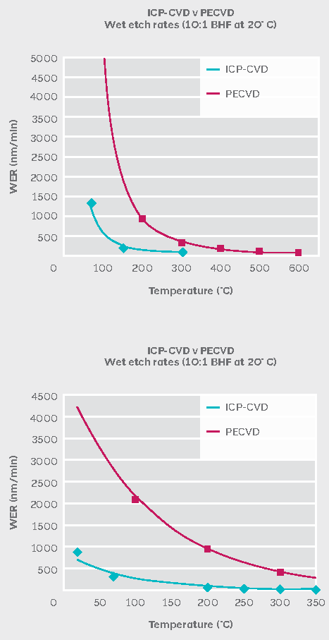
Using a PECVD process, Oxford Instruments Plasma Technology can produce uniform high-density films with minimal pinholes and low substrate damage whilst enabling the close control of material properties such as refractive index and stress. Usually, the film density quality is quantified for comparative purposes with wet etch rates (WERs), measured under standardised conditions using potassium hydroxide or buffered HF (buffered oxide etch - BOE). The WERs of SiO2 and SiNx films made by PECVD are given in Figure 7. Both films have relatively low WERs with deposition temperature >300°C. Moreover, considering the need for hydrogen-free deposition for the performance of certain InP devices, Plasma Technology provides optimised deposition process with minimized hydrogen content.
Laser Facet
For InP-based lasers, the edge-emitting facets are typically produced by cleaving along crystalline planes. An alternate approach is to form the mirrors by etching, which allows wafer-scale testing with probe cards and reduces manufacturing costs. It also allows for the decoupling of cavity length from chip size, thereby enabling significantly smaller cavities to be used, which in turn offers advantages for laser speed, controlling power requirements and heat dissipation in some designs. The etched facet needs to be smooth and vertical. A vertical profile is especially important to control the angle of emission of the light beam and to maximise the light output within the angle of light detection.
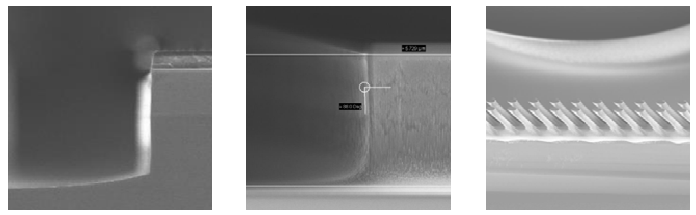
The dry etch process mentioned above based on chlorine/argon using Cobra® is a great solution to produce the laser facet, due to the high etch rate and vertical sidewall. Oxford Instruments Plasma Technology also provides a facet formation process with Chemically Assisted Ion Beam Etch (CAIBE), which has been proven to significantly reduce manufacturing costs. The Ionfab® delivers InP facet etching with ultra-high selectivity to achieve a vertical profile and reduce erosions in the top area of the waveguide. The embedded heating element enables high temperature processing to boost the etch rate. Furthermore, the substrate holder can rotate with precise angle control to support highly uniform etching and angled facet etching for certain vertical emitting lasers. Figure 8 shows the facet etching based on Oxford Instruments Plasma Technology's Cobra® and Ionfab®, with vertical and angled profiles.
Conclusion
With extensive InP device manufacturer relationships, Oxford Instruments Plasma Technology has established expertise in delivering optimum device performance and manufacturing efficiency. We have demonstrated plasma processing solutions designed to deliver the performance and yield demanded by the InP laser and photodetector markets. Our solutions have been proven to be low damage, superior quality, clean and highly reproducible.

