Products
DEPOSITION TOOLSPlasma Enhanced Chemical Vapour Deposition (PECVD)Inductively Coupled Plasma Chemical Vapour Deposition (ICPCVD)Atomic Layer Deposition (ALD)Ion Beam Deposition (IBD)ETCH TOOLSInductively Coupled Plasma Etching (ICP RIE)Reactive Ion Etching (RIE)Deep Silicon Etching (DSiE)Atomic Layer Etching (ALE)Ion Beam Etching (IBE)
Learning
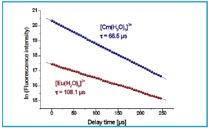
![Figure 3. Development of the solvated Eu(III) emission band as function of the delay time, [Eu(III)] = 1.8·10-5 mol L-1 in 0.01 mol L-1 HClO4.](https://www.oxinst.com/assets/uploads/learning/fluorescence-lifetimes/sp_3_AP_3.jpg)
![Figure 4. Development of the solvated Cm(III) emission band as function of the delay time, [Cm(III)] = 1.0·10-7 mol L-1 in 0.01 mol L-1 HClO4.](https://www.oxinst.com/assets/uploads/learning/fluorescence-lifetimes/sp_3_AP_4.jpg)