Focused ion beam (FIB) cross-sectioning is a critical process in semiconductor research and manufacturing. Through precise, site-specific milling, it exposes sub-surface structures and interfaces for direct visualisation of complex device architectures (Fig. 1). This capability is essential for failure analysis, process control, and structural characterisation, particularly as semiconductor components continue to increase in complexity.
Electron imaging of FIB cross-sections is typically used to inspect exposed interfaces at micro- to nanometre-scale resolution. Because of the geometry of the cross-section, this often requires a high stage tilt, typically 50-55°. Although simultaneous elemental analysis by energy dispersive X-ray spectroscopy (EDS) is possible, the combined effects of trench geometry and stage tilt can substantially limit X-ray collection. In these cases, shadowing greatly restricts or even precludes the assessment of elemental distribution within cross-sections. As a result, the identity of contaminants, material diffusion, or thin barrier films may remain unresolved, even when the physical shape of a defect or layer is clearly visible in the electron image.
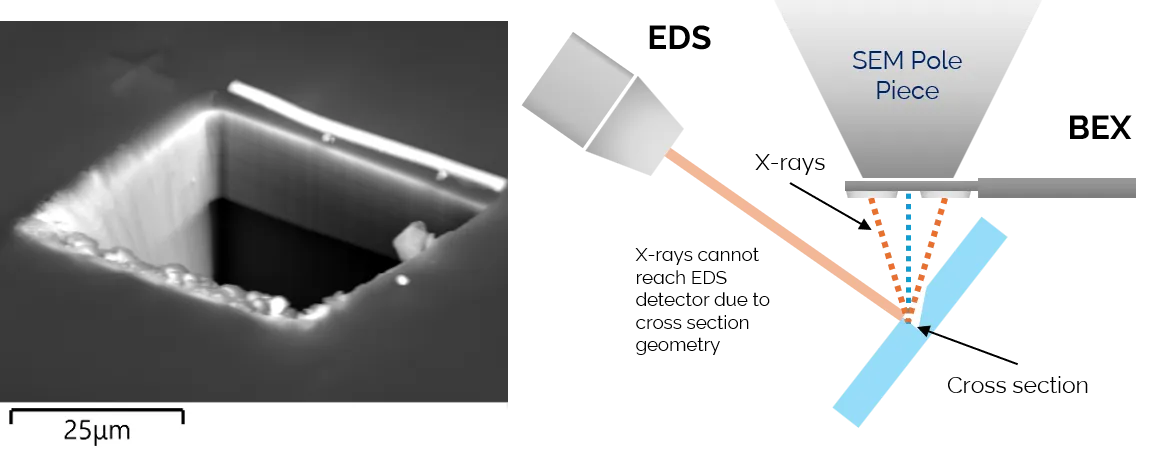
Figure 1. Electron image of GaN device cross-section, revealing 3D architecture of GaN device. Schematic highlights how the BEX insertion position overcomes X-ray shadowing problems associated with EDS.
BEX: A New Technique for Element Mapping of Cross-Sections
The introduction of the backscattered electron and X-ray (BEX) detector provides a new method for elemental characterisation of semiconductor cross-sections (Fig. 2). Positioned beneath the pole piece with a bird’s-eye view of the specimen, as opposed to the 35° angle of conventional EDS, the BEX detector greatly reduces shadowing effects that can compromise X-ray collection by EDS. This configuration enables high-speed elemental mapping directly within the cross-section, complementing EDS by extending the range of cross-sectional analyses that can be performed without complex sample reorientation, extended acquisition times, or lamella preparation.
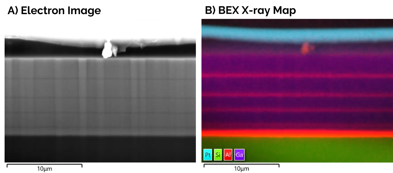 Figure 2. (A) Electron image of GaN device cross-section tilted at 45°. (B) BEX X-ray map of GaN device cross section.
In this example, a typical GaN device heterostructure on a silicon substrate, consisting of alternating layers of GaN and AlGaN, was analysed on a field emission scanning electron microscope equipped with a 100 mm Ultim Max ∞ EDS and the Unity BEX detector. EDS and BEX data were acquired simultaneously for 30 minutes at 12 kV, 3 nA beam current, and 45° stage tilt (Fig. 3). Under these conditions, the EDS Al map shows little of the device microstructure (Fig. 3A). In contrast, the unique geometry of BEX maintains X-ray collection from the cross-section, yielding 6 million Al X-ray counts compared with 0.1 million from EDS. This sixtyfold increase clearly resolves the AlGaN layers in the BEX map (Fig. 3B), demonstrating that BEX can recover elemental information where conventional EDS is geometrically shadowed.
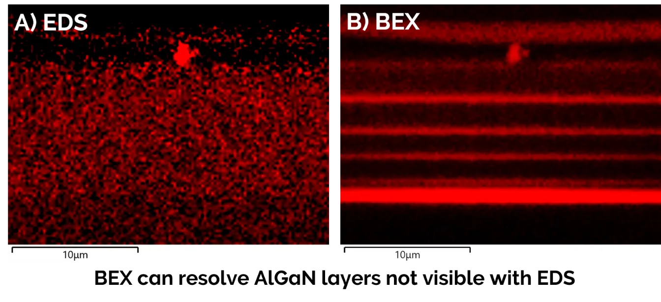 Figure 3. (A) EDS Al map of GaN cross-section. (B) BEX Al map of GaN cross-section.
Summary
BEX enables elemental characterisation of semiconductor cross-sections where trench geometry and stage tilt can limit conventional EDS analysis. Used alongside EDS, BEX extends the analytical value of established workflows by delivering high-count, spatially resolved elemental maps directly from challenging cross-sectional geometries. The result is a practical route to deeper device understanding, helping extract more insight and chemical understanding from every prepared cross-section.

