Introduction
Electron Beam Induced Current is a well-established analysis method of electrical activity in the SEM (and occasionally in the STEM). It provides a unique correlation of electrical and structural properties with very high spatial resolution. Typical applications include the identification of electrical defects in semiconductor devices (such as grain boundaries or single dislocations), as well as the measurement of non-radiative recombination activity and diffusion length of minority charge carriers.
Oxford Instruments' EBIC system is easy to install and use, with capabilities suitable for all experience levels. This integrated EBIC system with nanoprobing enables correlated microscopy, and EBIC analysis can be routinely performed alongside microanalysis techniques, such as EDS or EBSD, or used to guide sample preparation for TEM or atom probe tomography. The key and complex requirement of quantitative EBIC can be automatically managed during acquisition.
This application note shows how the Oxford Instruments' OmniProbe range of nano-manipulators is configured to provide an integrated EBIC microanalysis system. Typical images and quantification results from Si solar cells are included to explain the method and illustrate typical use. Potential configurations to fit particular needs are illustrated and options are highlighted where relevant.
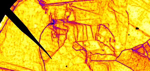
False colour EBIC map showing single dislocations, stacking faults, and grain boundaries in mc-Silicon material for solar cells.
Nanoprobing configurations
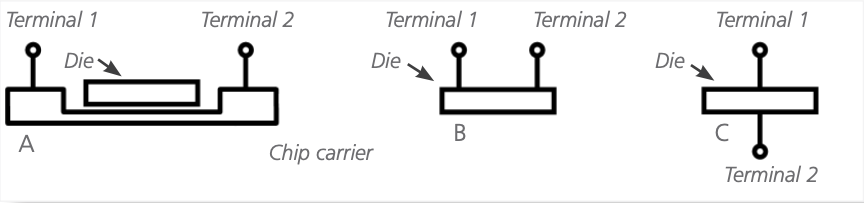
Fig. 1. Typical devices for EBIC characterisation.
A first EBIC requirement is to provide electrical connections to the device to be characterised. Almost exclusively, EBIC analysis is performed on two-terminal devices, i.e. diodes, which therefore demand two electrical connections. As illustrated in Fig. 1, a typical device may be a semiconductor die in a chip carrier (A), but most frequently they are a die with two top contacting points (B), or top-bottom contacts (C).
There are two possible configurations in which electrical probes can be used to provide these electrical connections, depending on the type of electrical measurements, as well as availability of an electrical connection to the sample stage in the microscope.
Where the chip carrier or the die provides two top terminals, the only possible probing configuration is the use of two manipulators (Fig. 2), preferably on opposite SEM ports. All Oxford Instruments' manipulators provide electrical connection from the probe to an electrical connector at the back of the manipulator, and therefore all can be used, including a combination of different nanomanipulators. This configuration brings the two electrical terminals, from the device mounted on the sample stage, out to connectors on the microscope column, and thus provides connections to the device test equipment.
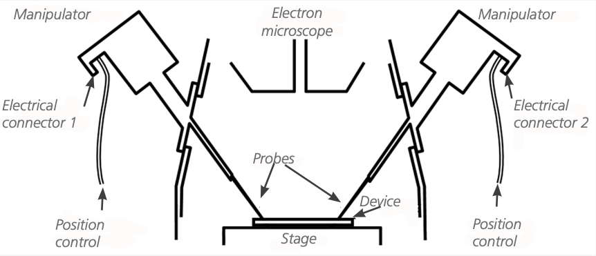
Fig. 2. Two-probe configuration for devices with two top terminals.
If the device has top-bottom terminals, and if an electrical connection to the stage is available from the microscope, then it is possible to achieve a second, simpler configuration based on a single probe. Provided that the electrical connection to the stage is shielded, then this single-probe configuration has the same performance as the two-probe configuration above. However, note that the stage touch alarm under this configuration must be disconnected when performing EBIC.
For the OmniProbe manipulators a coaxial shaft option (Fig. 3) is recommended for EBIC as it reduces noise under low beam current settings and also allows for high acquisition speeds. This option provides a probe that is held by an insulating gripper and connected to a coaxial cable, which is routed along the shaft to the electrical connector on the manipulator.
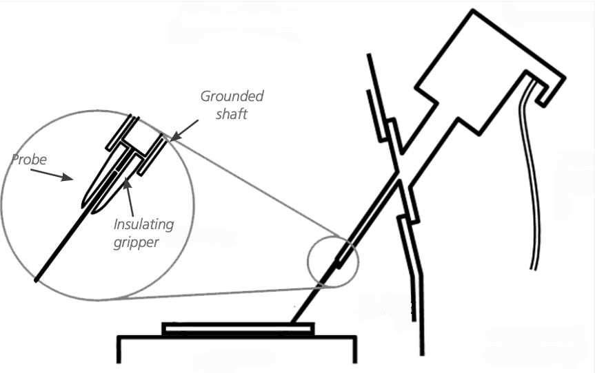
Fig. 3. Insulated probe-shaft configuration for the coaxial option.
Where the device is a die in a chip carrier, generally there is no concern over how the device may connect to the stage. If the device is a naked die, including top-bottom devices, then it is recommended that an insulating layer is used to support the device onto the stage to separate the back of the device from the touch alarm of the microscope.
It is important to note that the two-probe configuration can be used for top-bottom devices as well. In such situations it is recommended that a conductive piece is placed above a bottom insulating layer that supports the device, such that space is available to probe to the back of the device (Fig. 4). Conductive epoxy may be used to secure the sample, however this is not strictly necessary to provide electrical connections.
Overall, the two-probe configuration provides the highest performance and is most flexible: it does not require any further connections to the microscope stage, it does not interfere with the microscope touch alarm, and it does not need special shielding. It is also compatible with standard stages and any detectors which may occupy other ports, as well as lift-out in FIB-SEMs.
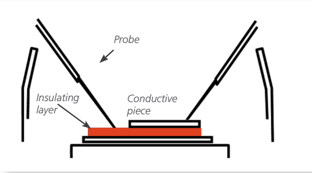
Fig. 4. Two-probe configuration for devices with top-bottom terminals.
It is also important to note that, where the SEM doesn't provide a suitable electrical connection to the stage, then a separate electrical feed through must be added to the microscope. Where applicable, Oxford Instruments will configure and provide a separate feed through such that the EBIC system is complete and ready for use.
EBIC characterisation of a multi-crystalline Si solar cell
An example of EBIC analysis of a multi crystalline Si solar cell is shown in Fig. 5 to illustrate typical results obtained using Oxford Instruments' technology. Devices were made from industrial multi-crystalline p-type solar material with top Schottky contacts and bottom ohmic contacts. Circular Al top contacts of 3 mm diameter were deposited away from the wafer edges, and the bottom contact was made with an Ag loaded conductive epoxy.
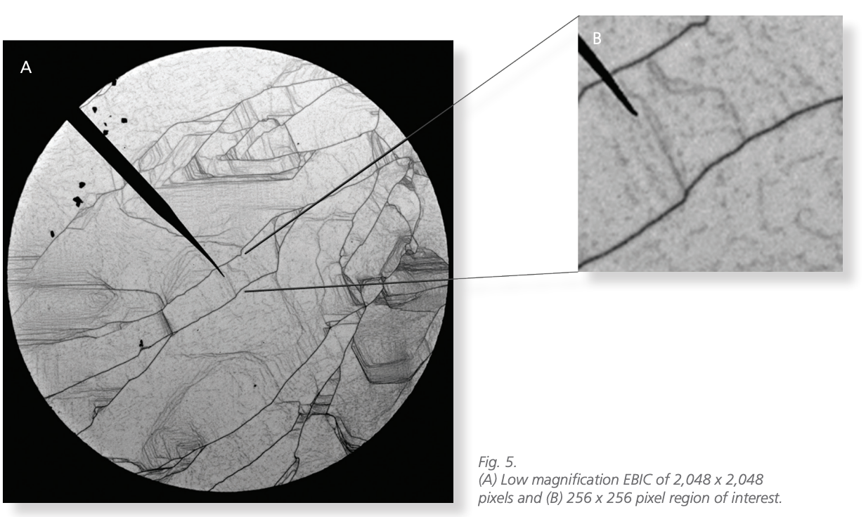
A single probe configuration was employed, where an OmniProbe 100 manipulator with the coaxial shaft was used for electrical connection to the top contact, and a stage connection was used for the bottom. The SEM acceleration voltage was 20 kV, with typical dwell times of 16 µs for 2,048 × 2,048 pixel images, and an EBIC amplification of 104 V/A.
I-V characteristics were recorded to confirm successful electrical probing and the diode behaviour of the solar cell device (Fig. 6).
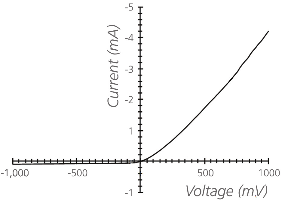
Fig. 6. Typical current voltage (I-V) characterisation of solar cell, showing good contacts and diode behaviour.
As illustrated in Fig. 6 above, the EBIC signal is collected only in the presence of the electric field of the circular Schottky contact, and the electrical probe produces a shadow, as the electron beam does not reach the device under the probe. A second low-magnification EBIC image recorded under the same conditions and presented in more detail is shown on the cover.
Changes in EBIC intensity can be quite subtle and difficult to see in grayscale, where human perception of small changes is rather poor. It is therefore common to apply a colour Look Up Table (LUT) where grayscale intensity is presented in a range of colours, for example from blue to red. This approach also enables an overlay of SE and EBIC signals where colocalisation is required, for example in Failure Analysis.
Grain boundaries and single dislocations are immediately presented in such EBIC images, where dark contrast corresponds to increased nonradiative recombination activity and therefore highlights active defects in the material. In this particular EBIC map, a majority of dislocations are perpendicular to the wafer, and therefore show as individual dark points, but some are at an angle or indeed parallel to the surface, and appear as elongated points or grey lines.
The dark contrast related to increased nonradiative recombination activity at dislocation cores extends away from the defects with an exponential decay, reflecting the diffusion length of minority charge carriers. Contrast of dislocation relates to recombination strength, and can be measured from such images. Depending on the relative dimensions to the diffusion length, this may also be convoluted with the beam size and electron interaction volume. A higher magnification image in Fig. 7 shows individual dislocations more clearly. This also shows that dislocations have the tendency to bunch or line up and that higher magnification is needed to distinguish dislocations that are close together.
As required for quantification, the acquisition system preserves a linear relationship between induced current and image intensity. The presence of the probe shadow is advantageous, as it provides an area of dark signal (no induced current) that is required for quantitative measurements. EBIC acquisition was thus calibrated before data acquisition such that image intensity in the area of the probe shadow is zero. Data was exported at 16-bit for further analysis.
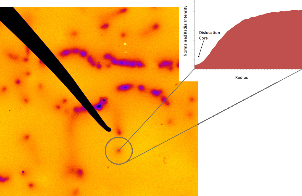
Fig. 7. Higher magnification EBIC image.
Analysis Method
A custom image analysis method was designed to automatically identify dislocations for these images, in particular for images captured at about 1,000x magnification. Identification may be used under a very wide range of magnifications; however, a lower magnification allows for analysis of many more dislocations in the larger field of view, and thus provides improved statistics. A limit at very low magnifications is imposed by the sampling required to image single dislocations; a limit at very high magnifications is given by the need to record signal away from the dislocation capture radius.
Criteria for automated identification of single dislocations include:
- an intensity in the middle of the dislocation core area that is smaller than the average background area intensity by significantly more than the background standard deviation
- a minimum circularity parameter when segmented by intensity
- no significant annular variation in intensity of the background area.
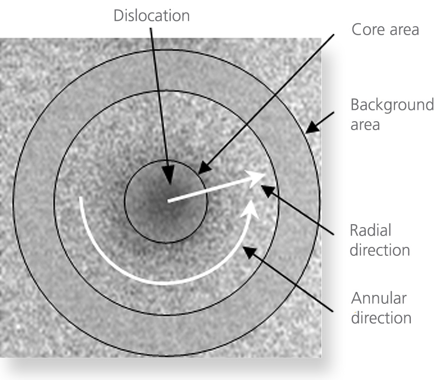
Fig. 8. Schematic diagram of areas used for automated identification and analysis of dislocations.
This approach (illustrated in Fig. 8) is designed to provide a natural feature segmentation for typical EBIC images, and thus to distinguish between single dislocations, grain boundaries and shadow of the tip. Further, the algorithm will reject from analysis dislocations partially obscured by the tip, or too close together.
Once dislocations have been identified, dislocation contrast C was calculated using the standard formula:
C = (Ibackground – Icore) / Ibackground
where Icore is minimum signal at the dislocation core and Ibackground is the mean background signal. Note that the calculated dislocation contrast is independent of the SEM contrast and brightness settings.
Results
The criteria described above have shown excellent discrimination of image features arising from recombination at dislocation sites and other contrast mechanisms, including grain boundaries, surface contamination and tip shadowing. Significant changes in background intensity have been observed between grains, and use of local background intensity has been found to be essential.
It has been found that a minority of dislocation sites are excluded from analysis, depending on the particular search values used in the automated algorithm. In particular, dislocations that are in close proximity to each other do not allow for adequate reading of the background intensity, and were excluded from the final analysis. However, the algorithm allows for identification of the large majority of dislocations.
The smallest measureable contrast value for this experiment was 0.01, which may be improved with longer acquisition times or reduced acceleration voltage. This level of contrast provides excellent discrimination for the purpose of this study.
The distribution of dislocation contrast has been measured for wafers from the bottom, middle and top of an ingot, respectively, and show a clear gradual shift in activity at dislocation sites as the ingot is solidified (see Fig. 9). Dislocation contrast average value is decreasing from 0.12 for the bottom wafer, to 0.10 for the middle wafer and finally to 0.08 for the top wafer. Overlapping distributions highlight here the importance of statistical analysis.
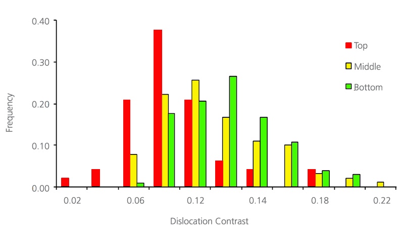
Fig. 9: Distribution of dislocation contrast
Automated analysis of dislocation contrast on solar cell wafers revealed that the EBIC contrast of dislocations is shifting from 0.12 at the bottom of the ingot to 0.08 at the top of the ingot. This shift in dislocation contrast may be assigned to the different total times available for dislocations to collect impurities, where dislocations at the bottom of the ingot have more time compared with those at the top.
However, this may also be attributed to the different densities of dislocations along the height of the ingot, where impurities at the bottom of the ingot are spread between a reduced number of dislocations, as compared with those at the top.
As highlighted by the overlapping distributions, such analysis and observation can only be provided by statistical analysis of dislocations, where automated identification is key. This study has proposed and demonstrated one such algorithm for automated defect identification.
Conclusion
Oxford Instruments provides an integrated EBIC hardware and software system with nanoprobes for electrical probing and automated quantitative signal acquisition. A number of nanoprobing configurations with port-mounted nanomanipulators are introduced and explained.
Application to typical mc-Si solar cell devices reveals grain boundaries, stacking faults and single dislocations. Quantitative acquisition and data export is used for automated identification and analysis of single dislocations, showing a statistical distribution of dislocation contrast. Analysis of devices from different heights of a single ingot reveal a shift in recombination activity from 0.12 at the bottom to 0.08 at the top.
Changes in dislocation contrast are attributed to varying dislocation density, or the different times available for dislocation to collect impurities along the height of the ingot, and therefore the resultant variations in impurity concentration at dislocation cores.
We thank Shark Lotharukpong and Prof. Peter Wilshaw from the Department of Materials, University of Oxford for their assistance in making this application note.

