Electron Backscatter Diffraction (EBSD) provides crystallographic and microstructural information from crystalline
materials in the scanning electron microscope. This FAQ answers common questions about EBSD principles, Kikuchi
patterns, sample preparation, measurement conditions, resolution and related diffraction techniques.
Click here to navigate within the article.
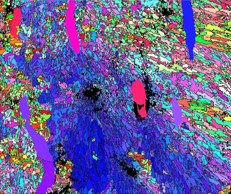
EBSD orientation map revealing the mineral architecture of the stony coral Montastraea cavernosa.
Fundamentals & Kikuchi patterns
What is EBSD?
Electron Backscatter Diffraction (EBSD) is a Scanning Electron Microscope (SEM) technique used to determine the
crystallographic structure, orientation, and phase of materials. EBSD analyses Kikuchi diffraction patterns, which are
generated when an electron beam interacts with a crystalline sample. The analysis provides detailed maps of grain
orientation, grain boundaries, texture, and phase distribution. It is widely used across research and advanced
manufacturing to understand material microstructure-property relationships.
Learn more about EBSD on ebsd.com
How does EBSD work?
In EBSD, an electron beam is directed at a crystalline sample tilted by approximately 70° inside the SEM. The
interaction between the electron beam and the sample generates backscattered electrons that form a Kikuchi diffraction
pattern. This pattern is captured by an EBSD detector and indexed by processing software to determine the crystal
orientation and phase at that measurement point. By scanning the electron beam across the sample surface and
collecting a diffraction pattern at each position, EBSD generates crystal and phase maps for the region of interest.
What is EBSD used for?
EBSD is used to characterise crystallographic orientation, grain size, texture, strain, and phase distribution in
crystalline materials. It provides valuable crystallographic and microstructural information that helps researchers
and manufacturers understand how materials form and behave. EBSD is applied in metallurgy, geology, semiconductors,
additive manufacturing, and failure analysis, and is widely adopted for R&D and quality control in academic and
industrial environments.
What materials can be analysed using EBSD?
EBSD can be used to analyse crystalline solids, including metals, ceramics, minerals, and semiconductors.
Non-crystalline materials such as glass do not produce Kikuchi patterns and therefore cannot be analysed using EBSD.
Material characteristics such as atomic number, crystal structure, and sample quality influence EBSD signal strength
and the SEM operating conditions required for reliable results.
What are Kikuchi patterns and how are they formed?
Kikuchi patterns are diffraction patterns that form when backscattered electrons interact with crystal lattice planes
inside a material. As the electrons satisfy Bragg’s condition during scattering, they form characteristic diffraction
bands that correspond to specific crystallographic planes. These patterns, often referred to as Electron Backscatter
Patterns (EBSPs), are projected onto the EBSD detector and captured for analysis. The geometry of these bands reflects
the crystal symmetry and orientation, which the EBSD software can reconstruct.
Read more about Kikuchi pattern formation here.
How does EBSD software analyse Kikuchi patterns?
EBSD software uses Kikuchi patterns and the known acquisition geometry of the measurement to determine the crystal
orientation and phase of a material. To do this, it identifies diffraction bands within the measured Electron
Backscatter Patterns (EBSPs) and compares their angular relationship with crystallographic reference data stored in a
database. This approach is commonly known as Hough-based indexing.
More advanced indexing methods can also use diffraction band intensities and compare the entire pattern with
reference patterns to improve accuracy and robustness.
Learn more about EBSD pattern indexing here.
What determines the quality of an EBSD pattern?
The quality of an EBSD pattern depends on several factors, including sample preparation, material properties,
acquisition settings, and SEM operating conditions. Higher accelerating voltages and a clean, flat, and damage-free
sample surface generally improve diffraction band contrast. Detector sensitivity and noise performance also play an
important role in capturing high-quality diffraction patterns suitable for reliable indexing.
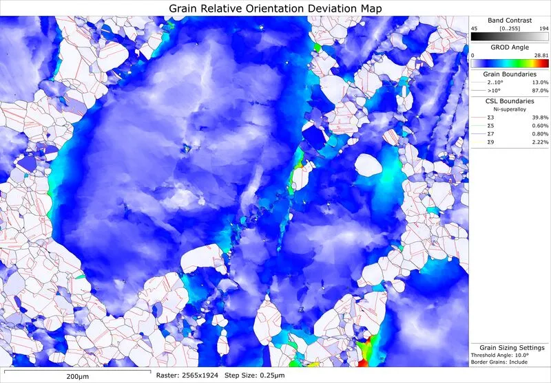
EBSD grain orientation map of nickel, revealing crystallographic orientation variations across the
microstructure.
Sample preparation and measurement
Why does EBSD require sample tilt?
A high sample tilt increases the number of backscattered electrons that reach the EBSD detector. Typical EBSD
experiments are performed with the sample tilted between 65° and 75° relative to the incident electron path. A higher
tilt angle increases backscattered electron yield and improves diffraction pattern quality. However, increasing the
tilt also reduces spatial resolution. The selected tilt angle is therefore a practical balance between diffraction
signal strength and spatial resolution.
What are best practices for EBSD sample preparation?
To obtain high-quality EBSD patterns and ensure reliable indexing, a clean, flat, and deformation-free sample surface
is critical. Best practice for EBSD sample preparation includes careful cutting, mounting, grinding, and mechanical
polishing to remove deformation layers. Final vibratory, electrolytic, or ion polishing can further refine the
surface. Poor sample preparation reduces the quality of EBSD results regardless of detector capabilities.
Learn more about sample preparation for EBSD on ebsd.com.
Does EBSD require sample etching?
Chemical etching is not inherently required for EBSD but is sometimes used in metallurgy to remove residual
deformation or reveal phases during preparation. The essential requirement is a flat, damage-free surface that is
often achieved by mechanical polishing and final ion-beam finishing rather than etching.
Can EBSD be performed on rough or non-flat samples?
EBSD can technically acquire data from slightly uneven surfaces, but significant roughness introduces geometric
distortions that degrade Kikuchi pattern clarity and reduce indexing accuracy. Local height variations cause
inconsistent band projection across the field of view, making the results less reliable. For quantitative mapping and
high-resolution analysis, a uniformly polished, flat surface remains essential.
Is EBSD destructive?
EBSD is generally regarded as non-destructive because the electron interaction is confined to a shallow region at the
sample surface. However, the technique requires intensive sample preparation, including polishing steps that modify
the surface layer but do not affect the bulk material. Some applications may require Focussed Ion Beam (FIB)
preparation or sectioning for site-specific or subsurface analysis, but these interventions remain highly localised.
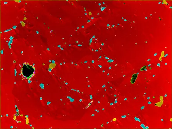
EBSD Steel phase map.
Interaction volume and resolution
What is the interaction volume in EBSD?
The interaction volume in EBSD refers to the near-surface region of the sample where the electron beam generates
backscattered electrons that contribute to the measured diffraction patterns. Its depth is typically limited to a few
hundred nanometres or less and depends on the electron beam’s accelerating voltage, material density, and the atomic
number of the elements present.
What is the spatial resolution of EBSD?
Spatial resolution refers to the smallest feature size that can be resolved in an EBSD dataset. The physical spatial
resolution of EBSD is governed by the size of the interaction volume, which depends on the accelerating voltage and
diameter of the electron beam, sample tilt and material density. For a given sample, reducing the accelerating
voltage, probe current or sample tilt can improve spatial resolution by reducing the interaction volume.
However, the effective spatial resolution observed in a dataset does not depend solely on the interaction volume. It
is also influenced by the software’s ability to analyse overlapping patterns, pattern quality and acquisition step
size. This means that the effective spatial resolution of an EBSD map is typically better than the separation of
adjacent interaction volumes alone.
What is the angular resolution in EBSD?
Angular resolution describes the precision of crystallographic orientation measurements. It depends on pattern
quality, pattern pixel resolution, and EBSD indexing algorithms. High-quality patterns and advanced indexing methods
improve angular precision. This is critical for analysing low-angle boundaries, misorientation and strain, and for
distinguishing orientations that could otherwise cause pseudosymmetry errors.
How does detector resolution affect EBSD results?
Detector resolution, expressed as the number of pixels in an electron backscatter pattern, influences the accuracy
and robustness of EBSD pattern indexing. Higher pixel resolution enables improved band detection and orientation
measurements, which is particularly important for complex or low-symmetry materials. However, higher resolution can
reduce acquisition speed, so the appropriate balance depends on the analysis objective.
Practical considerations and related techniques
How long does EBSD acquisition take?
EBSD acquisition time can range from seconds to several hours, depending on the measurement objective and
experimental setup. Key factors include the size of the mapped area, step size, and detector acquisition speed. Modern
EBSD detectors can acquire hundreds to thousands of patterns per second, supporting rapid collection of large
datasets. SEM operating conditions, such as beam current, and sample quality can also influence acquisition time, as
longer exposure times might be required to achieve sufficient pattern quality for reliable indexing.
To help plan measurements, some EBSD software, such as AZtec, include optimisation tools that estimate acquisition
time from the selected experimental parameters.
Can EBSD be combined with other electron microscopy techniques?
Yes, EBSD is often combined with other SEM-based techniques to provide complementary microstructural information. One
of the most common combinations is EBSD with Energy Dispersive X-ray Spectroscopy (EDS), which links crystallographic
and chemical information. EBSD is also frequently used alongside Forward Scatter Electron (FSE) imaging to provide
orientation and microstructural contrast information. It can also be combined with Focussed Ion Beam (FIB) milling for
three-dimensional EBSD or site-specific cross-sectional analysis and with in-situ
techniques to study microstructural changes during an experiment.
Effective correlative analysis requires an SEM configuration that supports all relevant modalities. Some SEM
platforms support simultaneous data collection from multiple detectors through optimised detector design, positioning,
and integrated software workflows.
What is TKD and how does it differ from EBSD?
Transmission Kikuchi Diffraction (TKD) is an SEM-based diffraction technique related to EBSD that is used to analyse
very fine-grained and nanocrystalline materials. Unlike conventional EBSD, where diffraction patterns are generated by
backscattered electrons, TKD uses electrons transmitted through a thin sample to generate Kikuchi patterns. This
significantly improves spatial resolution and enables crystallographic analysis at the nanoscale.
Read more about TKD here.
What is RKD and how does it differ from EBSD?
Reflected Kikuchi Diffraction (RKD) is a diffraction technique related to EBSD in which the sample is not tilted, and
the detector is positioned above the sample, near or around the pole piece. Like EBSD, RKD analyses Kikuchi
diffraction patterns generated from electron interactions within a crystalline material. However, this geometry
produces a significantly weaker diffraction signal than conventional EBSD at a sample tilt of approximately 70°. Its
main benefit is the ability to work with larger samples as the RKD setup does not require samples to be tilted and
thereby is not limited by space around the pole piece.
Key takeaways
- Electron Backscatter Diffraction (EBSD) provides crystallographic orientation, grain, texture and phase
information from crystalline materials in the SEM.
- EBSD analyses Kikuchi patterns generated by interactions between an electron beam and a crystalline sample.
- Clean, flat and deformation-free sample surfaces are essential for high-quality patterns and reliable indexing.
- Spatial resolution, angular resolution and acquisition speed depend on the sample, SEM conditions, detector
settings and analysis method.
- EBSD can be combined with techniques such as EDS, FSE imaging and FIB milling to provide complementary chemical
and microstructural information.
Learn more about Electron Backscatter Diffraction on ebsd.com.

