Introduction
An important part of the research and development of thin-film solar cells is the characterisation of microstructural and compositional properties of the functional layers. For this purpose, energy-dispersive X-ray spectrometry (EDS) and electron backscatter diffraction (EBSD) represent techniques which exhibit spatial resolutions on the nanometer scale but can be, at the same time, applied on large areas of several square millimeters. The application of EDS and EBSD is demonstrated on this example of thin-film solar cells with Cu(In,Ga)Se2 absorber layers. While EDS provides elemental distributions even in layers with a nominal thickness of 30–50 nm, EBSD gives not only information of average grain sizes, local orientations and grain boundaries. Moreover, strain distributions within individual grains can be calculated by the evaluation of EBSD patterns recorded on individual grains.
Thin-Film Solar Cells
Thin-film solar cells can reach power-conversion efficiencies of up to almost 21 % when using polycrystalline Cu(In,Ga)Se2 absorber layers [1] with average grain sizes of typically 0.5–1.5 µm at layer thicknesses of about 2–3 µm. A scanning electron microscopy (SEM) image of such a solar cell in cross-section including its mode of operation is given in Fig. 1.
One of the open questions in research and development of Cu(In,Ga)Se2 solar cells is why such excellent photovoltaic performance is possible in spite of the large densities of grain boundaries, which are normally considered as positions of enhanced recombination of the generated charge carriers. For the study of this issue, it is essential to determine the position of grain boundaries and to classify them according to their symmetries. Here, electron backscatter diffraction (EBSD) is a useful tool, which can be combined with other electrical and optoelectronic characterisation techniques on identical regions of interest for correlative analyses of extended structural defects in the thin-film solar cells.
The In and Ga distributions perpendicular to the substrate are not constant but exhibit gradients, which has a considerable impact on the optical properties of the Cu(In,Ga)Se2 layer since CuInSe2 has a different band-gap energy (1.04 eV) than CuGaSe2 (1.68 eV) [3]. For the measurement of these gradients and generally for the detection of elemental distributions and present phases in the thin-film stack, energy-dispersive X-ray spectrometry (EDS) is employed.
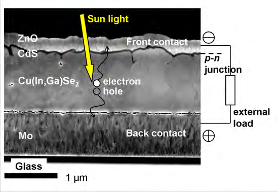
Fig. 1: Scanning electron micrograph of a thin-film solar cell consisting of a n+-ZnO/n-CdS/p-Cu(In,Ga)Se2/Mo/glass stack, as well as its mode of operation. Upon illumination by sunlight, electron-hole pairs are generated, mainly in the Cu(In,Ga)Se2 absorber layer, and separated when reaching the space-charge region of the diode (not shown here). The resulting charge densities at the ZnO and Mo contacts can be used to operate an external load. From Ref. 2.
Experimental Procedure
EDS elemental distribution and EBSD maps in the present work were obtained using an X-Max® 80 X-ray detector and a NordlysNano camera from Oxford Instruments on a Zeiss UltraPlus scanning electron microscope. The acceleration voltages and beam currents applied were 15 kV and 250 pA (EDS) or 55 nA (EBSD). Data acquisition as well as evaluation was performed using the AZtec® software package. Evaluation of stored EBSD patterns for strain/stress analysis within individual grains was conducted by use of the CrossCourt 3 software (BLG Productions).
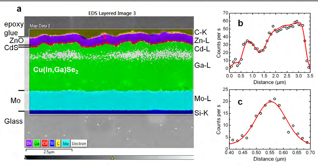
Fig. 2: a) Composed EDS elemental distribution maps, superimposed on a SEM image, using C-K, Zn-L, Cd-L, Ga-L, Mo-L, and Si-K signals. Extracted linescans of the Ga (b) and Cd distributions (c). The measured values (open circles) were fitted (red lines) using a FFT filter (b) and a Gaussian distribution with full width at half maximum of about 110 nm (c).
Results
Elemental distribution maps can be acquired on cross-sectional specimens of Cu(In,Ga)Se2 solar cells by means of EDS in a scanning electron microscope. By reducing the electron-beam energy to a minimum and by using only low-energy X-ray lines, the spatial resolution of the EDS signals can be improved substantially, to below 100 nm. In Fig. 2a, the elemental distribution maps using the C-K, Zn-L, Cd-L, Ga-L, Mo-L, and Si-K signals are given superimposed on a SEM image. All functional layers in the solar-cell stack, also the about 50 nm thin CdS layer, can be clearly identified. The extracted linescans of the Ga (Fig. 2b) and Cd signals (Fig. 2c) corroborate this capability, reproducing well the spatial distributions of the elements.
Complementarily to EDS, the solar-cell cross-sections are also studied by means of EBSD. Thus, the positions of grain boundaries (Fig. 3a) and the local orientation distributions of individual grains (Fig. 3b) in a CuInSe2 thin-film can be determined. Moreover, by recording and evaluating the EBSD patterns [4], strain distribution within individual grains can be computed (given for the strain tensors ε11, ε22, ε33 in Fig. 3c–e). A critical issue for this analysis is the determination of the reference point (actually the position of zero strain, which does not exist in a polycrystalline thin film), which is given as black spot in the middle of the highlighted grain in Fig. 3c–e. The average strain values were found to be about 3–5×10⁻⁴.
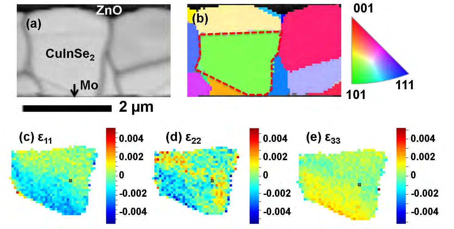
Fig. 3: EBSD pattern-quality (a) and orientation-distribution maps (b), acquired on a cross-section of a ZnO/CdS/CuInSe2/Mo/glass stack, with the local orientations given as false colors, see legend. Spatial distributions of the strain components e11 (c), ε22 (d), and e33, across the grain highlighted by dashed line in (b).
The sectioning function of a focused-ion beam (FIB) machine can be combined alternatingly with EBSD map acquisitions. From the resulting data acquired on a CuInS2 thin film, 3D EBSD cubes were reconstructed (Fig. 4). This 3D data provides not only structural information about individual grains but also gives direct access on how grain boundaries progress in depth of the layers. It is therefore possible to reproduce the 3D grain boundary network in the CuInS2 thin film.
This is very helpful when combining EBSD with electrical or optoelectronic analysis performed in SEM using electron-beam-induced current (EBIC) or cathodoluminescence (CL) measurements, with the aim of analyzing the impacts of grain boundaries on the optoelectronic properties and on the device performances of the corresponding solar cells. EBIC and CL exhibit much larger information depths than EBSD, which often makes the interpretation of combined EBSD/EBIC/CL data from identical specimen areas difficult, with respect to the influence of the microstructure on the EBIC and CL signals (see, e.g., Refs. 5, 6, 7). This obstacle can be avoided by acquiring a 3D EBSD cube after EBIC and CL measurements.
An example of combined EBSD and EBIC analysis on the identical position of a cross-sectional specimen of a Cu(In,Ga)Se2 solar cell is given in Fig. 5. The EBIC signal is enhanced in the space-charge region of the p-n junction of the solar cell owing to field-driven charge carrier collection within this region. Such measurements at (random) grain boundaries in identical Cu(In,Ga)Se2 thin films yielded increased and decreased EBIC signals [6, 9, 10] at different grain boundaries.
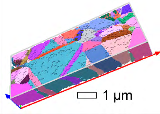
Fig. 4: Three-dimensional EBSD data cube, reconstructed from 20 individual two-dimensional EBSD maps acquired in plan-view on a CuInS2 thin film (deposited on Mo/glass substrates). The distances between the individual slices removed by focused ion beam (and in the presence of XeF2 ) were about 100 nm. Figure taken from Ref. 8.
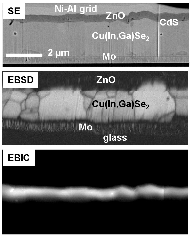
Fig. 5: Secondary-electron (SE) image, EBSD pattern-quality map, as well as EBIC image (at 10 kV and 200 pA), all acquired on the identical position of a cross-sectional specimen prepared from a ZnO/CdS/ Cu(In,Ga)Se2 /Mo/glass stack. From Ref. 2.
Conclusion
Structural and compositional analyses of the functional thin-films and their internal interfaces in Cu(In,Ga)Se2 solar-cell stacks can be performed at the submicrometer scale by means of EBSD and EDS in a scanning electron microscope. Modern instrumentation provides the means for high-speed measurements on large regions of interest in the 100-µm scale. It is very useful to combine these analyses with further electrical and optoelectronic characterisation in SEM on the same identical specimen positions, in order to provide direct access to structure–property relationships in semiconductor devices based on thin-film stacks.
References
- P. Jackson, D. Hariskos, R. Wuerz, W. Wischmann, M. Powalla, phys. stat. sol. (RRL), doi: 10.1002/pssr.201409040.
- D. Abou-Ras, J. Kavalakkatt, M. Nichterwitz, N. Schäfer, S. Harndt, A.J. Wilkinson, K. Tsyrulin, H. Schulz, F. Bauer, The Journal of The Minerals, Metals & Materials Society (JOM) 65 (2013) 1222–1228.
- M.I. Alonso, K. Wakita, J. Pascual, M. Garriga, N. Yamamoto, Phys. Rev. B 63 (2001) 075203-1-13.
- A.J. Wilkinson, G. Meaden, and D.J. Dingley, Mater. Sci. Techn. 22 (2006) 1271–1278.
- D. Abou-Ras, U. Jahn, J. Klaer, M. Nichterwitz, T. Unold, H.-W. Schock, J. Appl. Phys. 107 (2010) 014311-1-8.
- J. Kavalakkatt, D. Abou-Ras, J. Haarstrich, C. Ronning, M. Nichterwitz, R. Caballero, T. Rissom, T. Unold, R. Scheer, H.W. Schock, J. Appl. Phys. 115 (2014) 014504-1-10.
- M. Müller, D. Abou-Ras, T. Rissom, F. Bertram, J. Christen, J. Appl. Phys. 115 (2014) 023514-1-6.
- D. Abou-Ras, B. Marsen, T. Rissom, F. Frost, H. Schulz, F. Bauer, V. Efimova, V. Hoffmann, A. Eicke, Micron 43 (2012) 470–474.
- M. Nichterwitz, D. Abou-Ras, K. Sakurai, J. Bundesmann, T. Unold, R. Scheer, H.W. Schock, Thin Solid Films 517 (2009) 2554–2557.
- M. Kawamura, T. Yamada, N. Suyama, A. Yamada, and M. Konagai, Jpn. J. Appl. Phys. 49 (2010) 062301-1-3.

