Introduction
Certain applications in 3D sensing of VCSEL technology require higher power operation than Data Communication applications. As a result, there is a drive to produce high power VCSEL arrays of varying size and density depending on the combined output power required. However, multiple challenges such as cost control and thermal crosstalk between VCSELs arise when producing high power arrays. In addition, challenges also occur in the process of fabrication of VCSELs. As the density of the arrays increase, better process control becomes critical to deliver performance and cost.
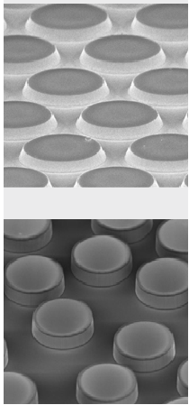
VCSEL array with varying density
Discussion on the Impact of Dry Etching on Demonstrating Reliable Performance at Low Cost
Dry etching of the VCSEL mesa is one of the critical steps within the process of fabrication of VCSEL. The mesa structure confines the light and exposes the high Al content layers for the oxidation process afterward. The mesa structure is formed by etching the top DBR stack. During this process, the control of the diameter of the mesa is important to define the size of the apertures. The sidewalls also have to be clean and smooth to prevent non uniformity of the aperture. In addition, it is critical to control the end layer across the full wafer size.
The end layer affects the electro optical performance, the yield and the reliability of the device.
Performance and Yield
Electrical performance such as the threshold voltage are defined by the total resistance between contacts and therefore the path of the current within the device. As the current travels, it is important to precisely identify each electrical interface. The accuracy of the etching depth determines one of these interfaces as it allows selecting the layer within the epi stack which will serve as an electrical interface. Across a full wafer, accuracy of the etching depth also helps maximising the yield as every VCSEL array needs to have similar electrical behaviour.
Reliability
Reliability is affected by thermal cycling of the device due to the different thermal coefficients of the oxide apertures. Controlling the etching depth and therefore having control over the end layer, gives manufacturers control over the layers exposed during the oxidation process.
Gaining Control over Process Performance
The selection of the end layer results from the combination of good uniformity of the etching depth across wafer as well as an endpoint detection system. In addition, achieving uniformly low footing gives a superior control over the selection of the end layer. One can achieve excellent uniformity of the etching depth but still have poor control over the end layer because of large non-uniform footing.
The uniformity of the etching depth across the wafer size depends on the exposed area. The etching depth at the centre of the wafer tends to be lower than the edge and this phenomenon increases as the wafer size increases. The etching process of GaAs/AlGaAs is a chemically driven process which is highly affected by the availability of ions and radicals across wafer. Excellent plasma ions distribution is therefore required to achieve good uniformity.
The etching detection system tracks the etching during the process with laser endpoint (LEP) typically used by VCSEL manufacturers. Oscillations in the intensity of the light due to multiple reflections at the DBR pair interface allow detection of each layer within the DBR. This method gives data on a single point of the wafer which can be extrapolated to full wafer data. Alternatively, Optical Emission Spectroscopy (OES) can also be used for endpoint detection. This method characterizes the etching depth over the full wafer using the concentration of etching by products in the plasma.
Footing is a common characteristic of highly chemical dry etching processes. To control footing, the general approach is balancing the chemical reactions occurring at the wafer surface during the etching process. This can be achieved through various methods which includes adjusting the gas breakdown in the plasma or the ion energy.
Demonstration of Highly Controlled Mesa Processing
Oxford Instruments has demonstrated ultra-low footing on sloped and vertical mesa. The process is highly uniform across full wafer size up to 150 mm. The etching depth is precisely controlled which gives manufacturer superior control over the process yield. The results are demonstrated on VCSEL arrays of various densities with spacing between mesas down to 2 µm.
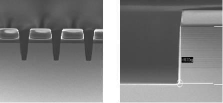
Low footing on emitter spacing < 2 µm, and controlled footing on sloped and vertical profile
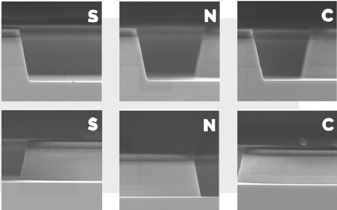
Controlled footing on sloped and vertical profile across wafer positions (S, N, C)
Conclusion
Multiple applications developed around 3D sensing are driving the compound semiconductor community to further enhance the process of fabrication of VCSEL devices. However key developments are required to bring this technology to maturity, bring the cost down and enable high volume manufacturing.
In order to meet requirements on performance, cost, yield and reliability, device manufacturers have to gain precise control of each step within the process of fabrication. The formation of the mesa is one of the critical steps within this process. To achieve high yield whilst delivering reliable performance, the etching depth must be precisely controlled across the full wafer size. In addition to endpoint technology commonly used to control the etching depth, low footing provides superior control over the process and supports a high number of good die per wafer. Low footing can be achieved by careful selection of the process conditions including chemistry and gas ratio. When ultra-low footing is demonstrated, the spacing between mesas within an array can also be reduced to less than 2 µm, hence enabling the fabrication of the highly dense VCSEL arrays required in new applications.

