Introduction
A full understanding of phase transformation processes is essential in order to refine processing conditions and to optimise the physical properties of a range of materials. This has become even more pertinent with the significant increase in importance of additive manufacturing, in which powders can be melted using electron or laser beams followed by phase transformations during the cooling process. Electron backscatter diffraction (EBSD) analyses of samples that have undergone phase transformations can provide a wealth of information about the grain-scale mechanisms that are active during the transformation process, and the recent development of parent grain reconstruction tools using EBSD data enables researchers to understand more about the high temperature microstructures.
However, there is nothing that can compare with direct observations of phase transformations as they occur. This poses a significant challenge for EBSD, since the higher levels of infrared (IR) radiation that occur above about 600°C can flood the EBSD detector signal. Here we present results collected from an in-situ heating experiment with simultaneous EBSD analyses on a pure Ti sample, using a new design of high T phosphor screen and the high-speed mapping capability and extreme sensitivity of the Symmetry S2 EBSD detector. The results show the efficacy of this approach for the detailed examination of high-T processes and, in particular, the α to β transformation in Ti.
Experimental Details
The experiments presented here were all conducted on a 7 x 10 x 1 mm commercially pure Ti sample. The sample was polished firstly using diamond paste down to 0.5 µm size and then with an additional step using colloidal silica (OPS). Finally, the sample surface was etched using a mixture of glycerine and aqua regia (HNO₃+3 HCl) for about 10 seconds. Electron backscatter diffraction patterns (EBSPs) were collected using the Symmetry S2 fibre-optic-based CMOS EBSD detector. The front of the detector was equipped with a new design of high T phosphor screen, with an in-built interference filter for effectively filtering out the incident IR-radiation resulting from the heating of the stage and the sample. In contrast to conventional high T phosphor screens that use a thick metal coating on the surface of the phosphor screen, the use of an interference filter maintains the excellent sensitivity of the Symmetry S2 detector, enabling high speed analyses using low electron doses even at high sample temperatures.
The experiments were performed using a Carl Zeiss Gemini SEM 450 field emission electron microscope. During all experiments the accelerating voltage was set to 20 kV with a beam current of about 25 nA, operating at a working distance of 16.7 mm. The microscope was equipped with a heating stage (Heating Module 1050°C, Kammrath & Weiss, Schwerte, Germany) capable of generating temperatures up to 1050°C. The temperature of the stage, Ts, was measured at the ceramic part of the stage which was in physical contact with the sample and was monitored during all experiments. The sample temperature, Tp, was derived from Ts by a linear interpolation from 0°C to the first appearance of the high temperature β-phase of Ti expected at 882.5°C according to the literature (M. K. McQuillan, 1963, Int. Metal. Rev. 8, 41–104). The temperature difference was determined to be 53°C at the phase transformation. The experimental setup in the microscope chamber is shown in Figure 1 at both ambient conditions and ~850°C Tp.
During the experiments the set-up of the Symmetry S2 detector was varied according to the experimental objective, ranging from high-speed and lower resolution EBSP collection with a 0.25 ms exposure time (for fast mapping at 4000 patterns per second (pps)) to the collection of high-quality EBSPs using the full megapixel resolution of the detector, with 25 ms exposure (i.e. 40 pps). The full details are provided in the individual sections below.
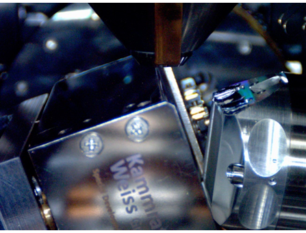
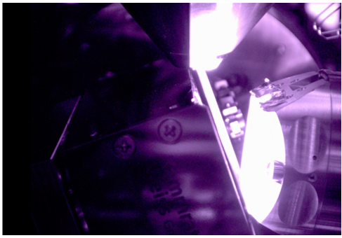
Fig 1. Measurement setup in the GeminiSEM 450 field emission electron microscope, imaged using the in-chamber camera. The heating stage is tilted 70° with respect to the electron beam towards the Symmetry S2 EBSD camera. Top: Setup at ambient conditions. Bottom: Setup at ~850 °C Tp showing the significant IR radiation.
Pattern Quality at High Temperatures
To test the functionality of the new high temperature phosphor screen we collected several patterns at different temperatures, camera exposure times and camera modes. Only a dynamic background correction was used: this allowed the investigation of the effects of any blemishes on the phosphor screen (such as pin-hole artefacts) on the final EBSP quality.
Typical results of these tests are presented in Figures 2–4. Figure 2 shows an α-Ti EBSP collected at 720°C Tp (prior to the phase transition), with and without the simulated indexing model. This was collected using the full detector resolution (1244 x 1024 pixels, "resolution" mode) with an exposure time of 2.5 ms and 10 frames averaging (equating to an electron dose of 625 nAms). Note the high pattern quality and the complete absence of any artefacts associated with increased IR radiation.
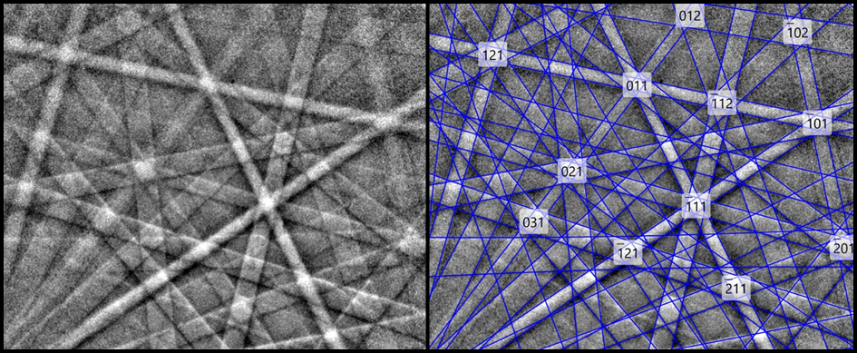
Fig 2. EBSP of α-Ti at ~720 °C sample temperature, collected with 1244 x 1024 pixels pattern resolution and displayed with the indexing solution overlay (solution mean angular deviation, MAD, = 0.18 °)
At 895°C Tp, following the onset of phase transformations, we collected a set of EBSPs from both α- and β-Ti and these are shown in Figure 3. For these EBSPs the detector was kept in resolution mode (1244 x 1024 pixels) but using a single frame at an exposure time of 0.9 ms, resulting in a total electron dose of 22.5 nAms. Even at this sub-millisecond exposure time, the EBSP quality remains very high and indexing was carried out with a very low mean angular deviation (MAD).
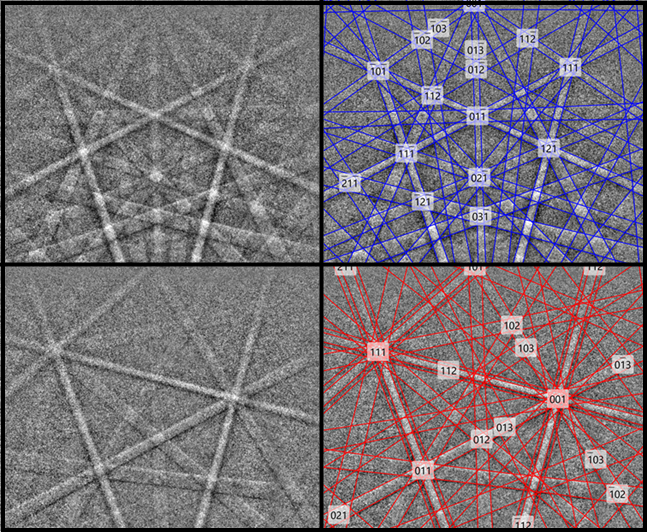
Fig 3. Typical EBSPs at ~895 °C sample temperature, collected using full 1244 x 1024 pixel pattern resolution with 0.9 ms exposure time. Top: α-Ti, MAD 0.13°. Bottom: β-Ti, MAD 0.11°.
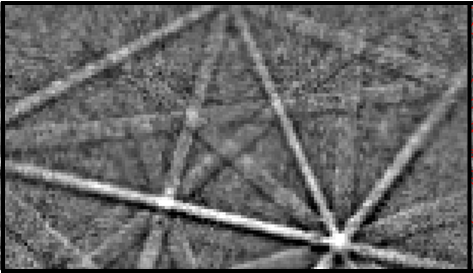
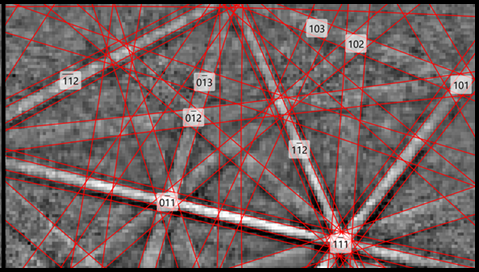
Fig 4. Typical EBSP of β-Ti at ~895 °C Tp, collected with 156 x 88 pixel resolution (Speed 3 mode) with 0.9 ms exposure time (MAD 0.27°).
In order to track dynamic processes during the heating experiment, it is necessary to maximise the data collection speed. For this we used the "Speed 3" mode of the detector, allowing us to collect EBSPs at speeds in excess of 4000 indexed patterns per second. The EBSP resolution is a lower 156 x 88 pixels, as shown in Figure 4, but the solid angle is still sufficient to get perfect indexing. The pattern shown here was collected with a 0.9 ms exposure, but during the experiments a 0.25 ms exposure was used, allowing maps with 900,000 points to be collected in under 4 minutes.
High Speed EBSD Mapping of the α-β Phase Transformation
The temperature Tp was increased in steps of 100°C from ambient conditions up to about 800°C. After reaching 800°C the temperature was increased in smaller steps of about 5°C up to a calculated sample temperature of about 920°C. EBSD maps covering an area of 760 x 570 µm were repeatedly collected with a measurement step size of 0.7 µm and at a mapping speed of ~4000 pps, each map taking under 4 minutes. To eliminate any shadowing of the EBSD detector phosphor screen caused by the shielding of the heating stage, we made use of the software controlled and motorized tilt function of the Symmetry S2 detector. The electron dose per pattern was ~6.25 nAms, and indexing was carried out using a Hough Resolution of 35 using 9 detected bands and giving indexing rates typically between 90 and 96%. Minor data processing was performed using AZtecCrystal, before relevant phase and orientation maps were created.
Due to the time resolution of 4 minutes per map, α/β-Ti linear transformation rates could be derived from the data. At 890, 900 and 905°C the rates were found to be 0.64, 0.86 and 2.6% per minute, respectively. Figure 5 gives an overview of the microstructural development through the α-β transition, noticeably demonstrating the initial formation of β-Ti along the α-Ti grain boundaries. The orientation data also enable an analysis of the orientation relationship between parent β grains and child α grains upon cooling, allowing us to test the efficacy of parent grain reconstruction algorithms. This is the subject of a separate application note.
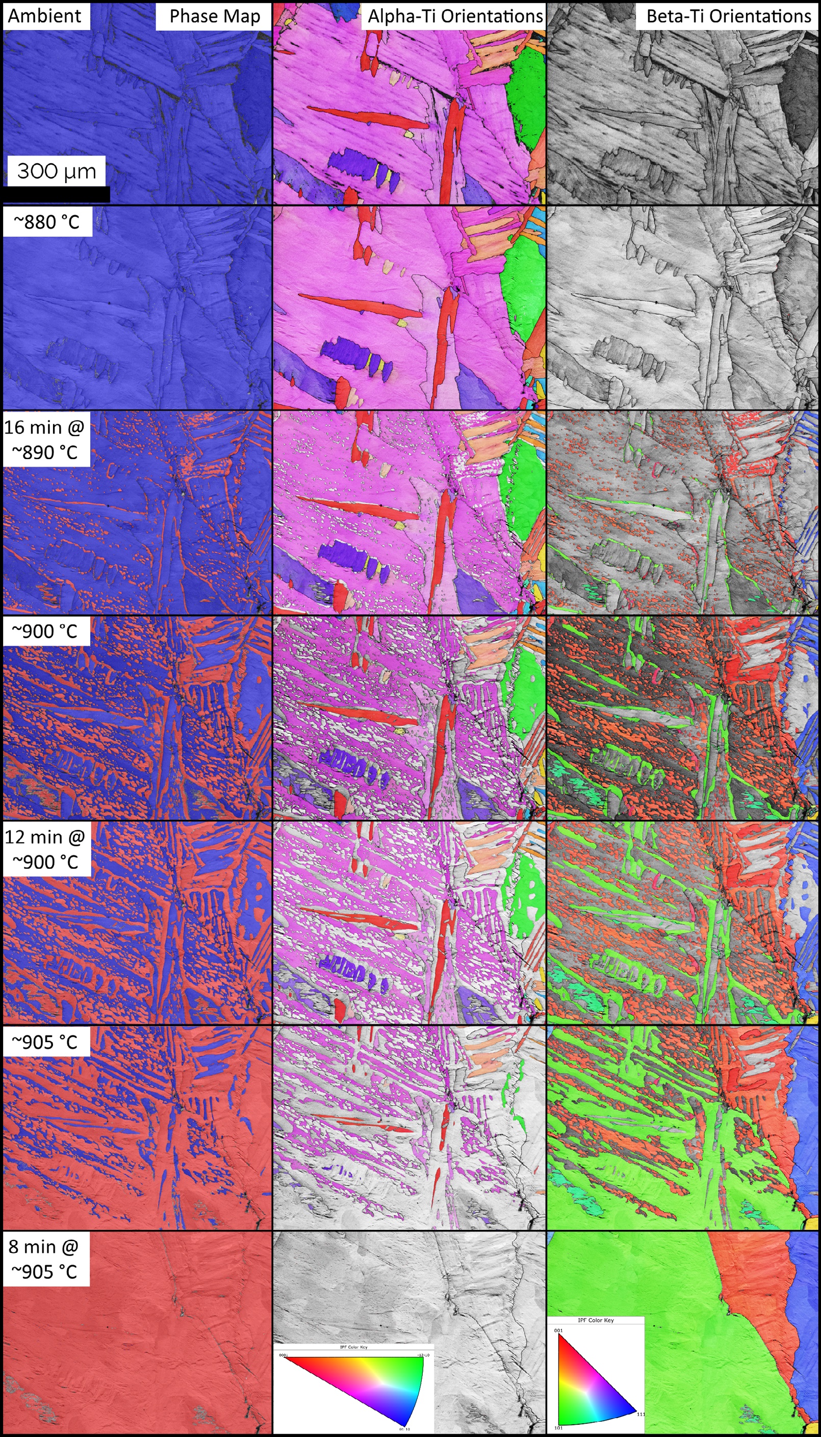
Fig 5. EBSD maps showing the microstructural and phase changes in Ti during a heating experiment. Left: Phase maps, with α-Ti in blue, β-Ti in red. Centre: Pattern Quality maps with α-Ti orientations coloured using the IPF-Z colouring scheme (see inset, bottom). Right: Pattern Quality maps with β-Ti orientations coloured using the IPF-Z colouring scheme (see inset, bottom). The sample temperature and duration held at that temperature (if relevant) are shown for each set of maps.
Summary
A new high temperature phosphor screen, utilising an interference filter, is available for the Oxford Instruments CMOS range of EBSD detectors, facilitating in-situ experiments up to temperatures of ~1000°C. The advantages of the new screen over conventional high-T screens are:
- Significantly improved sensitivity, enabling fast EBSD mapping at high temperatures using low beam currents and minimal loss of performance during conventional EBSD work
- No detrimental artefacts caused by imperfections on the phosphor screen (such as scratches or pin-holes). The increased IR signal at high temperatures results in such imperfections causing bright spots in conventional high-T screens, necessitating static backgrounds for all analyses. With the new design, the IR signal is removed even if the phosphor screen has blemishes, enabling the sole use of dynamic backgrounds through the whole temperature range
We demonstrate the performance of this new screen using heating experiments on commercially pure Ti at temperatures up to 1000°C. The quality of the patterns, even with short exposure times and low electron doses, is consistently excellent ensuring that indexing rates during EBSD mapping remain very high. In addition, the high sensitivity and fast collection speed of the Symmetry S2 detector permits the repeated collection of high resolution EBSD maps at short intervals throughout the experiment's duration. Here the transformation of α-Ti into β-Ti is effectively characterised, and the results can be used to further our understanding of high-T processing of Ti-based alloys.

