Introduction
Semiconductor technology is becoming increasingly important in global healthcare enabling novel understanding, discovery and treatment of disease to make healthcare more affordable and efficient, both in and out of the clinic. With the global healthcare industry being valued at US $1.65 trillion in 2016 and expected to reach US $2.69 trillion by 2025, it is an important growing industry. Key drivers behind this ongoing market growth are growing and aging populations, over urbanization, rising disease prevalence — all of which are putting further strain on healthcare systems already grappling with issues relating to access, quality, and cost. Convergence of technology from the seemingly disparate fields of semiconductor device processing and life sciences is fast revolutionising healthcare and medical research by enabling quick and accurate diagnosis. This in turn is increasing the speed and efficiency of treatment for various conditions as well as biomedical research and development.
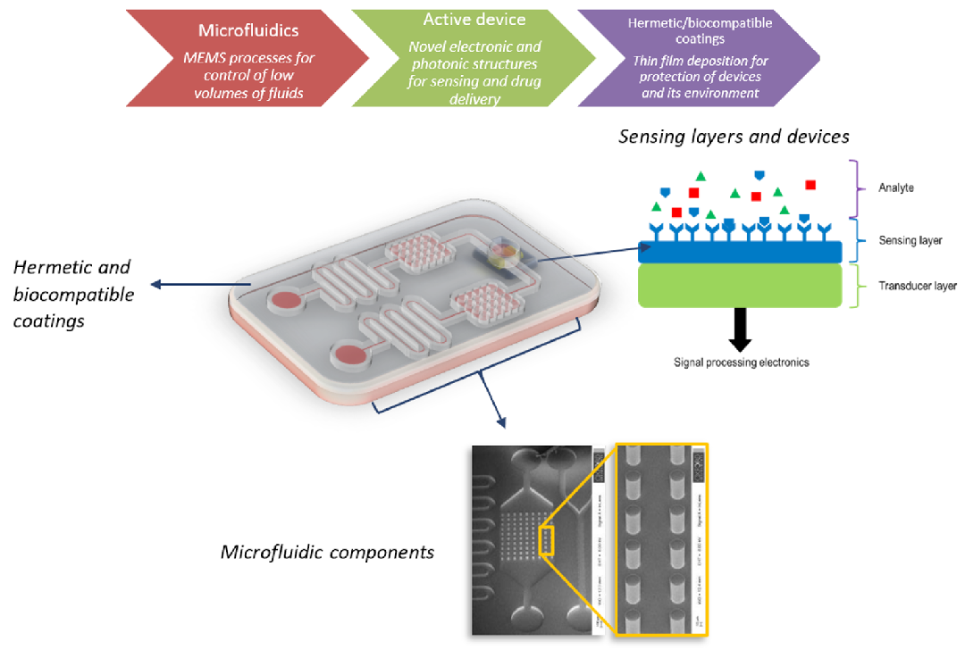
Fig. 1 — Major processing requirements for biomedical device fabrication
Previously…
In the previous editions of this white paper series we delved into the various aspects of plasma processing techniques for microfluidics fabrication and control of surface properties. These processes provide biomedical device engineers and scientists the protocols to design and tailor devices based on the application.
Sensor Fabrication: Electronic, Photonic and MEMS Based Devices
Biomedical devices are made up of microfluidics that perform the task of manipulating, processing and transporting analytes in a form that is ready to be processed by the active systems. These active components are commonly fabricated using semiconductor fabrication processes combined with surface functionalization techniques. Typically these systems consist of two key components:
- The sensing layer: This is normally based on a combination of organic or inorganic thin films and biologically active substances such as antibodies or antigens, nucleotides, cells, proteins, enzymes etc. This layer provides the specificity necessary to detect the species of interest in an analyte.
- Transducer: Interaction of the analyte with the sensing layer affects a change in the physio-chemical properties which the transducer layer converts to a measurable electrical, optical or any other physical signal that correlates with the concentration of the species of interest.
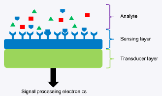
Fig. 2 — A generalized schematic illustrating the design of biosensing systems
The very first biosensor reported in 1962 by Clark and Lyons was an electrochemical system consisting of a membrane of an enzyme called glucose-oxidase which was combined with an oxygen electrode to yield the first glucose sensor. Owing to demands in control and monitoring of complex biochemical processes, both in-vitro and in-vivo, and driven by constant progress in life sciences and biomedical technology (genomics, proteomics and pharmaceuticals), combination of this with the immense miniaturization potential offered by semiconductor fabrication has resulted in the proliferation of these devices.
The Sensing Layer
A crucial component of the biosensor, the sensing layer specifically identifies target biomolecules within the analyte and induces a local electrical, chemical or physical change. The composition of this layer is specific to the function and type of biosensor being fabricated. Very often, materials with surface amphoteric groups are preferred as they enable links to appropriate functionalization. These layers are usually oxides (Example: SiO2, Al2O3, HfO2, Ta2O5) deposited by PECVD or ALD techniques, but also a wide variety of other materials have been researched depending on the sensing strategy and target. Sometimes, due to the nature of the substrate, the biosensor architecture or other device and economic constraints, it becomes necessary to deposit organic sensing layers like APTES in order to form linkers for antibody functionalization. Traditionally these layers have been deposited directly from liquids through Langmuir-Blodgett or similar liquid phase techniques. However, vacuum based CVD or PECVD techniques have proven to yield much denser and more homogeneous films.
Transducer Materials
The function of a transducer is to convert the physio-chemical change induced by the sensing layer into a signal that can be acquired and is suited for data analysis and storage. Most often used acquisition techniques use an electrical signal (Example: frequency or current change), a photonic signal (wavelength or phase change), or resonant frequency shift using MEMS structures (mass change).
Electrical Transducers
Electrical transducers mainly employ semiconductor thin-film-based devices such as Ion-sensitive Field Effect Transistors (ISFETs). Figure 3 illustrates a typical structure of an ISFET which is fabricated quite similar to a traditional MOSFET structure, replacing the gate with an electrolyte and a reference electrode. The sensing layer made up of the dielectric senses the change in the surface potential which in turn modulates the source-drain current. This type of device is very commonly used in pH sensing devices which are employed in a wide range of diagnostic devices including DNA sequencing.
A typical process flow for the fabrication of an electrical transducer based biodevice is illustrated in Figure 3. In this example a ZnO nanowire based transducer is fabricated on which an Al2O3 sensing layer is deposited. Here ZnO is deposited via remote plasma ALD on an Oxford Instruments FlexAL system using pulses of Di-ethyl Zinc (DEZ) and O2 plasma followed by an etch into nanowires using a Plasmapro ICP RIE system. This was followed by atomic layer deposition of the sensing dielectric layer Al2O3. Depending on the requirements of the device and the substrate these processes can be done using ICP/PE-CVD/CVD as well.
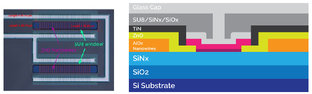
Fig. 3 — Fabrication of a ZnO transducer based ISFET with an Al2O3 sensing layer. Oxford Instruments offers solutions for several processes for such device fabrication. (Device image courtesy of Southampton University)
Photonic Transducers
Photonic devices for biosensing offer scalable fabrication and high sensitivities (pM–fM). Integrated photonic array structures are ideally suited to function as transducers for lab-on-a-chip applications. On-chip photonic components such as grating-couplers, interferometers, photonic crystals, microring resonators or slot waveguides are integrated to build such a device which detects analyte change by transduction into a change in wavelength or phase of the propagating signal.
Photonic biosensors take advantage of well-known fabrication processes in the semiconductor industry, thereby offering high levels of integration and mechanical stability while lowering production costs. Silicon is the material of choice for photonic biosensors along with Si based materials such as SiNx and SiO2. Latest strategies involve combination of Si based photonic structures with polymers and novel materials such as graphene.
Silicon based waveguide structures can be quite fine and need to exhibit high light confinement, coupling and minimal propagation losses. The main sources of optical loss stem from the cross-sectional morphology (such as sidewall angle, slope and roughness) and inherent material characteristics. Deviation from 90° side wall slope increases the scattering loss in addition to the roughness that could originate from mask issues and high ion energy bombardment. Low loss waveguide conditions with vertical slopes and low roughness have been achieved on Oxford Instruments solutions on the PlasmaPro platform as shown in Figure 4. Depending on the wavelength of operation and detection mechanism (only evanescent field interaction is discussed here), device fabrication process may involve deposition and etch of SiOx/SiNx layers as well. For example, silicon-on-insulator (SOI) loses transparency at wavelengths lower than 1100 nm which precludes its application in sensors. Si3N4 is a popular alternative which is transparent in the 700–1000 nm source band where water absorption and fluorescence is low and sources and detectors are less expensive. These dielectric layers can be deposited at very high quality using Oxford Instruments deposition platforms for PECVD/ICPCVD.
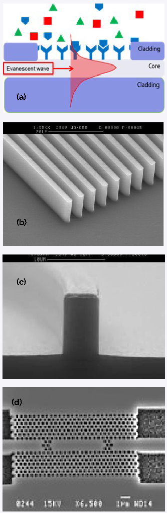
Fig. 4 — (a) Illustration of the photonic transduction mechanism using the evanescent wave interaction. (b)–(d) Various photonic structures etched using Oxford Instruments plasma etch solutions.
Membranes and Cantilever Based Devices
Micro-cantilevers: These types of extremely sensitive MEMS structures are able to locally perform label-free molecular recognition measurements with high resolution. The transduction principle is based on simple mechanical bending or change in vibrational resonance in the cantilever upon a sensing event on its surface. This nanomechanical motion is usually read out using an optical or piezo-resistive transduction mechanism. Oxford Instruments have developed several process solutions for the creation of such cantilevers and membranes using deep silicon etch techniques to overcome challenges due to a decrease in lateral heat dissipation from the etching structures on a membrane. This occurs due to lower surface area available for heat management during etching. In several biosensing applications these membranes or cantilevers need to be coated with an appropriate sensing layer and therefore require low damage high density film deposition processes. Using ICPCVD and ALD techniques on the PlasmaPro and FlexAL platforms very high quality thin films can be achieved. ALD provides the unique advantage of being able to provide uniform conformal coatings across these structures to ensure even loading and allowing deposition of extremely thin films to ensure minimal changes in the quality factor (and therefore sensitivity).
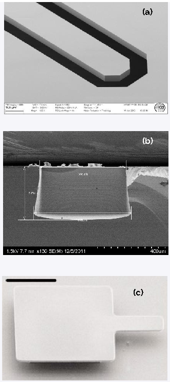
Fig. 5 — (a–b) MEMS cantilevers and membranes etched using Oxford Instruments Bosch deep silicon etch. (Figure (a) courtesy of CIS Erfurt.) (c) 90 nm thin Si3N4 cantilever coated with ALD SiO2 to enable chemistries for biochemical functionalization.
DNA Sequencing Using Microfabricated Membranes
Facile and inexpensive DNA sequencing technologies with the ability to unravel information from entire genomes rapidly not only have the potential to revolutionize the world of medicine and technology, but also facilitate advances in fundamental studies in life sciences. Historically, this has been achieved through multiple biochemical reactions and fluorescence based readouts. Over the last decade significant advances have been made in next generation sequencing (NGS) technologies which use optical methods like those commercialized by Illumina and Pacific Biosystems. Here, glass offers a significant advantage due to its favourable optical properties especially as development in this technique is pushing the limits of detection, and optical figures of merit such as background fluorescence and scattering become even more critical. With increases in cost per genome, demands are pushing well below the $1000 per genome towards $100; the current approach is to go fluorescent-label free. The most successful approaches in this space have integrated high aspect ratio nanopores with a direct electronic detection method for sequencing, such as those commercialized by Oxford Nanopore, Genia Roche, Quantum Biosystems etc., which are the drivers for application of silicon over glass for microfluidic components in these devices.
Nanopore sequencing works on the principle of translocating DNA through a nano-aperture embedded within a membrane. This is a label-free approach that produces electrical signals specific to each base that allow identification of corresponding sequences. Current commercially available devices for nanopore sequencing use protein based nanopores like α-hemolysin produced using programmed bacteria. While these have been very successful in proving the viability of this technique for DNA sequencing, solid state nanopores (and hybrid ones) are touted to bring the next jump in improving costs, durability, stability and scalability of this powerful technique.
Solid state nanopore sequencing requires the fabrication of extremely thin suspended structures using semiconductor fabrication techniques. Early efforts involved creation of holes in silicon nitride membranes using Ar ion milling techniques. Since then several materials and detection mechanisms have been explored using artificial nanopores using materials like SiO2, SiC and Al2O3 films. More recently, novel layered materials with superior mechanical and electrical properties such as graphene, boron nitride (BN) and molybdenum disulfide (MoS2) are being investigated as membranes. These atomically-thin membranes with thickness in the order of the size of the DNA nucleotide (~0.3 nm) are expected to significantly improve spatial resolution and lower error rates.
Fabrication of membranes using thin films of materials like SiO2, Si3N4 and Al2O3 require careful control of film stress and quality. This can be achieved by controlling plasma enhanced deposition parameters like pressure, temperature, power, choice of plasma source etc. via Oxford Instruments PECVD and PE-ALD solutions. In addition to thin-film deposition techniques, plasma technology also provides solutions for the fabrication of several novel materials not only for synthetic membranes for DNA sequencing but also for several electrical/optical transducer devices:
- Silicon, Germanium and ZnO Nanowires: These can be fabricated via CVD using nanoparticle catalysts in the Nanofab system as well as via top-down approaches using RIE/ICPRIE of SOI on our Plasmapro systems.
- Carbon Nanotubes: Grown using either CVD or PECVD on metal catalysts at elevated temperatures.
- Graphene and other 2D materials: These processes require very high temperatures and are deposited via CVD and ALD processes.
- Thin film oxides (e.g. TiO2, Ta2O5, Al2O3 etc.)
Conclusion
Research and development in the last couple of decades have demonstrated a large number of applications and techniques for biomolecule sensing using semiconductor devices. These techniques have resulted in many options for sensor fabrication and integration based on sensing mechanism, target species and operation environment. This white paper gives an overview of Oxford Instruments Plasma Technology expertise for the wide variety of processes required in electronic, photonic or MEMS based sensors fabrication.
Next Time…
Application of biomedical devices outside the lab require them to be protected from variations in the environmental conditions surrounding the device. In some cases, like implantable devices, the environment — especially in-vivo applications — needs to be protected from device toxicity. The challenges can be overcome with a wide range of thin film coatings which serve several functions from acting as layers for surface protection and passivation to rendering the device biocompatible. In the next and final paper of this white paper series, techniques for coating such critical protective thin films will be discussed.
References
- Clark and Lyons, Annals of the New York Academy of Sciences, 102, 29, (1962)
- C.E. Nwankire et al., Analytica Chimica Acta
- 781, 54, (2013)
- Sun et al., Microelectronic Engineering
- 153, 96, (2016)
- Jain and Alam, arXiv: 1305.5729
- Waggoner et al., J. Appl. Phys.
- 107, 114505 (2010)
- https://nanoporetech.com/how-it-works/types-of-nanopores
- Li J, et al., Nature
- 412 166, (2001)

