Two-dimensional (2D) materials with remarkable electronic, optical, mechanical, and chemical properties attract
attention in fundamental scientific research due to their great potential for industrial application. In the past
decade, numerous papers have shown that Raman spectroscopy and imaging can reveal unique characteristics of 2D
materials such as electronic and optical properties that differ significantly from those of their respective bulk
precursors [1-5]. For example, bandgaps of semiconducting transition metal dichalcogenides (TMDs) can be tuned by
changing the number of layers, the chemical composition, or the strain of the materials.
The focus nowadays is on exploring and designing new materials by employing heterostructures consisting of stacks of
layered materials. Such heterostructures can be tuned based on their composition and stacking, thus combining the
advantages of different 2D material properties to designable quantum phenomena. Interlayer effects within the
heterostructure can also give rise to new quantum phenomena that are not present within the individual layers,
creating new fields of study for fundamental materials science research [2].
Raman spectroscopic imaging remains a fast, non-destructive and convenient technique for characterising the
properties of 2D materials at the laboratory level and mass-production scales. Raman imaging is used to check the
quality of 2D TMD materials in terms of number of layers, uniformity, and defects [1-5]. Resonant Raman effects
provide information about the optoelectronic properties and doping/vacancies of the TMD-materials. To excite resonant
Raman effects in TMDs, specific excitation wavelengths are required. Furthermore, the properties of the electronic
band structure can be analysed using luminescence measurements. Grain boundaries can be identified by second harmonic
generation. Ideally, such measurements are conducted with full polarisation control, as the properties of 2D materials
naturally are anisotropic.
The witec360 confocal Raman imaging microscope with its fundamentally modular design not only allows for the
acquisition of single Raman or photoluminescence (PL) spectra, but also confocal images of the highest resolution.
These lead to a comprehensive understanding of the phenomena occurring in 2D TMD materials. The edges of 2D crystals
often show different optoelectronic properties than the crystal and here the combination of Raman, PL, and second
harmonic generation (SHG) imaging can provide detailed information such as chirality, orientation, and symmetry. To
enable all of these different Raman, PL, and SHG measurements to be performed with one instrument, a spectrograph with
a large variety of gratings, such as the Hexalight spectrometer, is beneficial.
The aim of this application note is to highlight the benefits of the witec360 microscope with the Hexalight
spectrometer by presenting a series of Raman/PL/SHG measurements performed on a heterostructure deposited on a
Si/SiO2 substrate. The sample consists of triangular crystals of MoS2 and WS2 covered
with a graphene sheet.
Results and Discussions
Fig. 1a shows a white light image of the analysed heterostructure (graphene/WS2/MoS2). The
frame marks the area examined with Raman, PL, and SHG. The crosses mark the positions where Raman spectra were
acquired with different excitation wavelengths for MoS2 and WS2 (Fig. 1b, c respectively). For
both TMDs the in-plane (E2g) and out-of-plane (A1g) vibrational modes are highlighted. These
Raman bands change slightly to lower wavenumbers as the excitation wavelength is increased. For MoS2 (Fig.
1b) additional Raman bands arise at 451-460 cm-1 when excited with 633 nm. These bands are related to
strong electron-phonon coupling, leading to resonance enhancement involving longitudinal acoustic phonons at the M
point of the Brillouin zone (2LA(M) modes) when the laser energy is close to the material´s exciton states. For
WS2 the 2LA(M) mode arises at 350 cm-1 when excited at 532 nm and 633 nm.
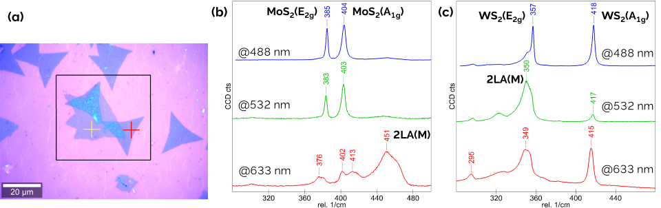
Fig. 1: (a) Bright-field image of the analysed heterostructure. The
frame marks the position of the Raman/PL/SHG images. The Raman spectra of MoS2 (b) were acquired from the
red and the WS2 spectra (c) from the yellow marked positions, respectively, using different excitation
wavelengths. Spectra acquisition parameters: integration time: 0.5 s, 10 accumulations, spectrograph setting: 1200
g/mm.
Characterisation of the graphene top-layer
Differences are observed in the Raman spectra of the top-layer graphene due to the underlying heterostructure. Fig. 2
shows the colour-coded Raman image of the graphene layer covering the analysed heterostructure (a) and the
corresponding Raman spectra (b). To acquire the Raman spectra of the graphene, the 300 g/mm grating is required in
combination with the 600 mm Hexalight spectrometer and TrueComponent Analysis (TCA) was used to identify the different
regions.
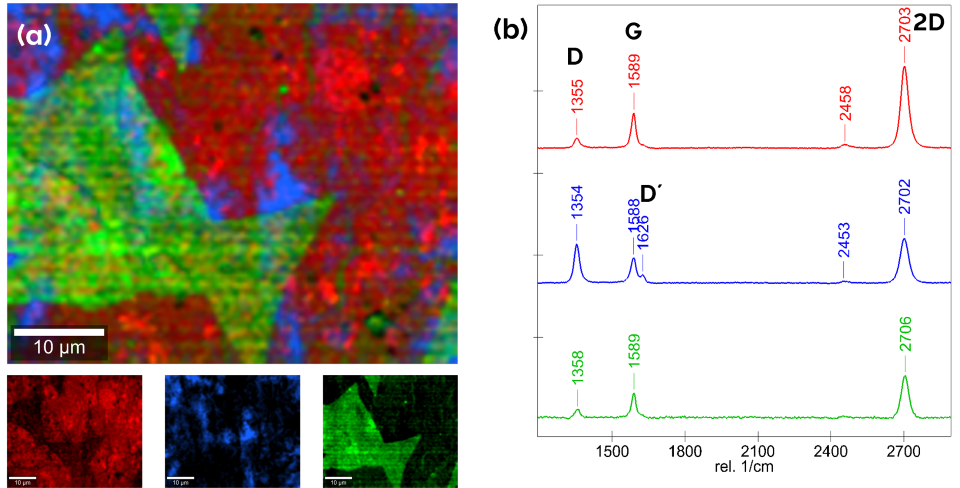
Fig. 2: False
colour-coded Raman image of the graphene layer (a) and Raman spectra evaluated using TCA (b). The smaller images at
the bottom show the corresponding distributions used for the overlay image. Measurement parameters: λex:
488 nm, power: 1.0 mW, objective: 100x/0.9, area: 50x40 µm2, 150x120 pixel, integration time: 100 ms/pixel.
The graphene-specific Raman bands are the D-band at 1356 cm-1, the G-band at 1590 cm-1, the
D´-band at 1623 cm-1, and the 2D-band at 2704 cm-1. All spectra in Fig. 2 show an intense D-band
and the presence of the D´-band, indicating a defect-rich graphene layer on top of the TMDs. Lorentzian fits were
performed for all four characteristic Raman bands of graphene, and characteristic intensity ratios (areas under the
peaks) were calculated for the analysed sample area.
These are summarised in Table 1:
- The ID/IG ratio provides information about the defect density in the graphene layer and is
inversely proportional to the crystallite size [6].
- The ID/ID´ ratio is sensitive to the type of disorder present, making it particularly
relevant for graphene-based composites that often exhibit diverse defect chemistries due to functionalisation, edge
exposure, or matrix interactions. According to [7] a value of 3.4 corresponds to boundary-like defects (e.g., grain
edges).
With a value of 3.3 for the I2D/IG ratio, the graphene layer can be considered a monolayer with
a high defect density.
| |
ID/IG |
ID/ID´ |
I2D/IG |
FWHM (2D) |
| Monolayer graphene |
0.38 |
2.28 |
4.09 |
38.5 cm-1 |
| Graphene/MoS2/WS2 |
0.33 |
0.67 |
2.50 |
24.5 cm-1 |
Table 1: Summary of the results of the Lorentzian fit.
Raman charactersation of the TMDs
Using a high-resolution grating (2400 g/mm), the properties of the WS2/MoS2 triangles of the
heterostructure are analysed in more detail. With this grating, Raman images of the highest spectral resolution are
obtained. Fig. 3a shows a Raman image of the same sample area as in Fig. 2a, measured with 488 nm excitation. The
characteristic Raman bands of MoS2 and WS2 are shown in red and blue in Fig. 3a, b. For both
TMDs the in-plane (E2g) and out-of-plane (A1g) vibrational modes are highlighted. The Raman
image shows that the heterostructure consists of two triangles of MoS2 (blue) and an irregular flake of
WS2 (red). The purple colour reveals overlaying MoS2 and WS2 monolayers, whereas cyan
indicates WS2 bilayer. This result was obtained from TCA.
The spectra were also analysed using Lorentzian peak fitting of the in-plane (E2g) and out-of-plane
(A1g) vibrational modes of MoS2 (Fig. 3c, d). The images and histograms show blue shifts of the
MoS2 vibrational modes from pristine to overlayed with WS2. The (E2g) Raman band
provides information on the in-plane strain, while the out-of-plane mode (A1g) gives evidence of the
quality of the interfacial contact in the heterostructure. Furthermore, these images show that the two MoS2
triangles interact differently with the WS2 layer, leading to a higher blue shift of the A1g and
E2g Raman bands in the upper left triangle compared to the lower MoS2 triangle. This shows that
the orientation of the two TMD crystals strongly influences the Raman signal, and thus the optoelectronic properties.
This finding is more evident using advanced peak fitting.
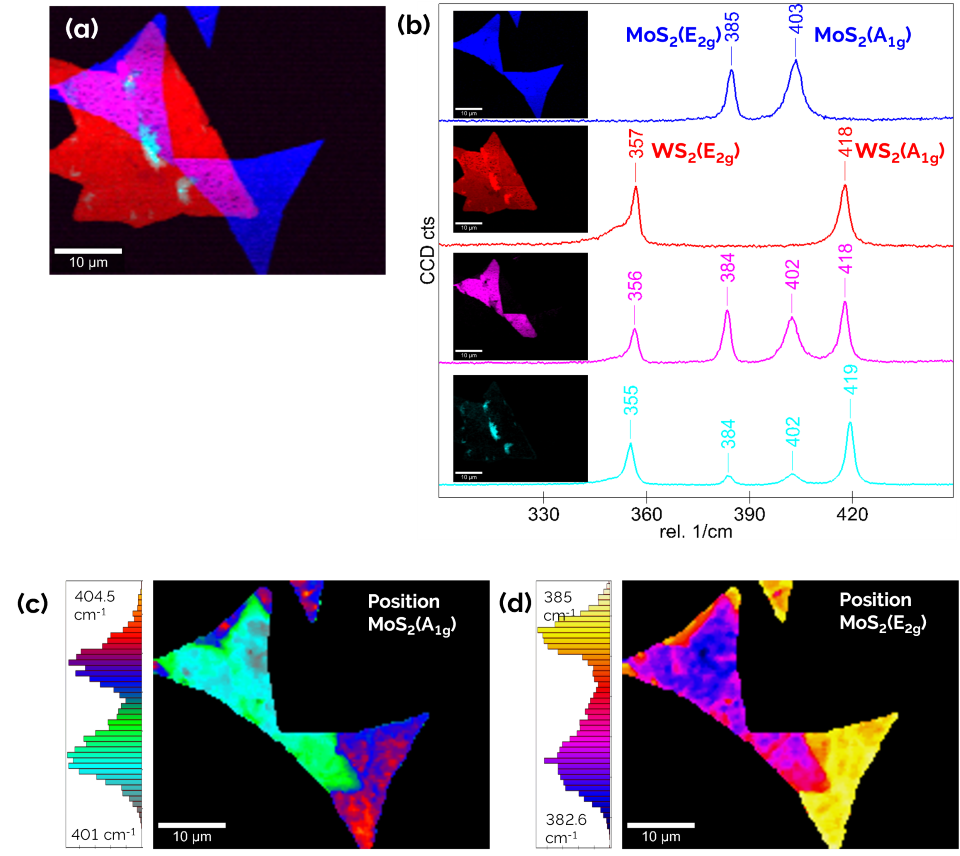
Fig. 3: False colour-coded Raman image of the TMD heterostructure
(a) and Raman spectra evaluated using TCA (b). Raman images and histograms of MoS2 triangles using
Lorentzian fits for the A1g (c) and E2g (d) Raman bands. Measurement parameters: λex:
488 nm, power: 1.0 mW, 100x/0.9 objective, 50x40 µm2, 150x120 pixels, 100 ms/pixel.
Fig. 4a shows the PL spectra of graphene/MoS2, graphene/WS2 and
graphene/WS2/MoS2 heterostructures. The PL in TMDs is dominated by the recombination of
electrons in the conduction band with holes in the spin-orbit split valence bands. There are two distinct emission
features: the ground state A exciton (A-exciton) between the conduction and upper valence band, and the higher energy
B exciton between the conduction and lower valence band. The strongest PL is measured for the graphene/WS2
heterostructure with a peak at 1.98 eV, characteristic for A-excitons. The graphene/MoS2 heterostructure
shows two broad PL peaks at 1.87 eV and 2.01 eV corresponding to the A and B excitons. The PL spectrum of the
graphene/WS2/MoS2 heterostructure (blue) shows a shift towards lower energies of the A-excitons
of the studied TMDs. The PL image of the graphene/WS2/MoS2 heterostructure shows a different
exciton energy of 1.94 eV, thus indicating a structure with different optoelectronic properties. This PL image was
obtained using a pseudo-Voigt function to fit the complete array of PL spectra.
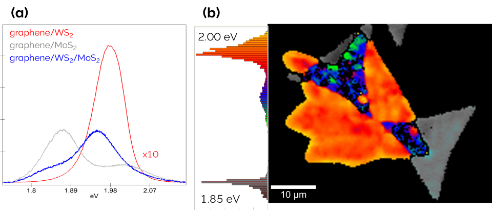
Fig. 4: PL spectra (a) and PL image of the heterostructure (b)
colours represent PL peak positions found from pseudo-Voigt fit of each PL spectra. Measurement parameters:
λex: 488 nm, power: 1.0 mW, 100x/0.9 objective, 50x40 µm2, 150x120 pixels, 100 ms/pixel.
Further information regarding properties of the heterostructure can be obtained by using laser energies which
generate additional Raman resonances. The 532 nm and 633 nm laser excitation generate a second-order Raman resonance
(R) in WS2 involving the longitudinal acoustic mode LA(M). This resonance results from a coupling between
the electronic band structure and lattice vibrations and is used to study the phonon-exciton interaction [8]. Fig. 5
shows the Raman image and changes in the Raman spectra which are unique to the 532 nm excitation wavelength. As
expected, the monolayer of WS2 shows the highest LA(M) intensity [8]. In the regions of the image, where
WS2 and MoS2 are overlapping, the LA(M) mode of WS2 reveals small differences which
can be visualised by applying the TCA to the array of spectra. This resonant mode is extremely sensitive to the
intralayer coupling, revealing also the defects in graphene covering the WS2 structure.
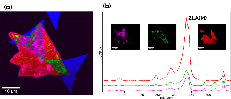
Fig. 5: False
colour-coded Raman image of the TMD at 532 nm excitation (a) and Raman spectra evaluated using TCA (b). Measurement
parameters: λex: 532 nm, power: 2.0 mW, 100x/0.9 objective, 50x45 µm2, 150x135 pixels, 100
ms/pixel.
At an excitation energy of 633 nm, both MoS2 and WS2 show the presence of the LA(M) modes. Fig.
6 shows the Raman image and Raman spectra acquired at this excitation wavelength. For MoS2, the LA(M) modes
appear as a broad Raman band in the range 420-470 rel. cm-1. The strongest signal is observed for the
MoS2 monolayer (blue colour). In the areas where MoS2 and WS2 are overlapping, this
resonant mode for MoS2 decreases, but reveals defects in the triple-graphene/WS2/MoS2
heterostructure region (magenta component). The LA(M) modes of WS2 show a shift towards higher wavenumbers
at the edge of the crystal (green component), revealing defects in the WS2 crystal or the overlaying
graphene sheet.
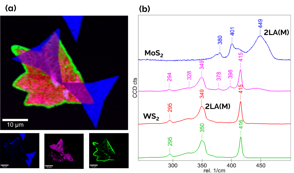
Fig. 6: False colour-coded Raman image of the TMD at 633 nm
excitation (a) and Raman spectra evaluated using TCA (b). Measurement parameters: λex: 633 nm, power: 30
mW, 100x/0.9 objective, 50x45 µm2, 150x135 pixels, 200 ms/pixel.
Finally, SHG measurements were performed to examine the heterogeneity of the WS2 monolayer. This imaging
technique uses a non-linear optical effect in which two photons with the same frequency interact with a material, are
combined, and generate a photon with twice the energy of the initial photons. SHG is sensitive to changes in crystal
orientation and symmetry. It can visualise grain boundaries and reveal strain fields by rotating the polarisation
direction of the excitation light. Fig. 7 shows SHG images acquired at 0o (a), 30o (b) and
60o (c) rotation of the polarisation of the excitation light with respect to the x-axis of the images. The
images show that the irregular WS2 sheet consists of several triangular crystals with different
crystallographic orientation. The polarisation curves (Fig. 7d) measured at the marked positions show the rotation
angle of the irregular WS2 crystals. Fig. 7e is an overlay of the defect Raman image (from Fig. 6 green
colour) with the SHG image (Fig. 7a), highlighting the sensitivity of the resonant Raman band of WS2 to
grain boundaries and defects. Fig. 7f is an overlay of the colour-coded Raman image from Fig. 6 measured at 633 nm
excitation with the SHG image (Fig. 7c). It shows the sensitivity of the Raman image to crystal orientation, strain
and defects.
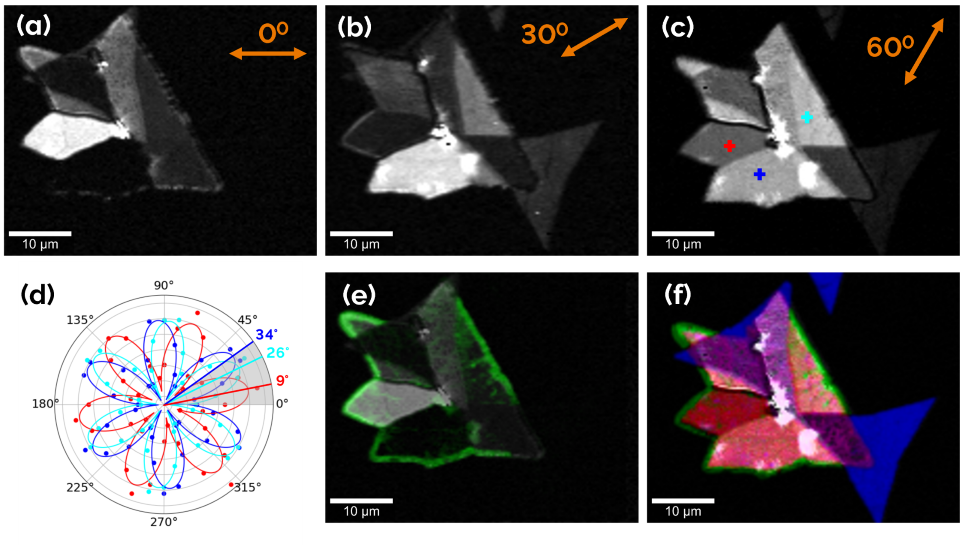
Fig. 7: SHG images of the heterostructure at different polarisation
angles of the incoming light: 0o (a), 30o (b) 60o (c). Polarisation curves (d) were
measured at the colour-coded marked positions in (c). Overlay of defects (e) and Raman (f) with SHG images.
Measurement parameters: λex: 1064 nm, power: 30 mW, 100x/0.9 objective, 50x45 µm2, 150x135
pixels, 100 ms/pixel.
Summary
A heterostructure consisting of triangles of WS2/MoS2 covered with graphene was analysed with
the witec360 confocal Raman imaging microscope. Correlative measurements were performed using different excitation
lasers and spectral gratings to highlight the influence of the excitation laser on the Raman measurements. To
characterise the graphene layer a grating covering the entire spectral range was used, whereas for the
characterisation of the TMDs a high-resolution grating with the proper blaze angle was selected. PL measurements on
the other hand require a low-resolution grating to cover the broad luminescence range. The Hexalight spectrometer with
its six-grating capability enables optimised spectroscopic conditions for all the laser wavelengths used. The
excitation laser was selected to encompass resonant Raman scattering across both TMDs. The measurements presented show
that resonant Raman scattering amplified first order and multi-phonon lattice vibrations under excitation energies
tuned to exciton transitions. Resonant confocal Raman imaging offers a high-resolution, non-destructive method to
probe phonon dispersion, electron-phonon coupling, and structural characteristics of heterostructures of 2D TMD
materials. Polarisation-dependent SHG measurements complete the correlative measurements, revealing that the
WS2 sheet consists of several triangular grains rotated in relation to each other.
Experimental Details
The witec360 confocal Raman imaging microscope was equipped with 4 lasers with excitation wavelengths of 488 nm, 532
nm, and 633 nm for Raman measurements, and a 1064 nm pulsed laser for SHG experiments. A Hexalight spectrometer (600
mm focal length) with the optimal grating combination was used for the measurements presented in this application
note. Further experimental details can be found in the figure captions.
References:
- Xin Cong, Xue-Lu Liu, Miao-Ling Lin, and Ping-Heng Tan, npj
2D Materials and Applications (2020) 13.
- S. Novoselov, A. Mishchenko, A. Carvalho, and A. H. Castro Neto, Science 353 (2016) No 6298.
- Gatensby, N. McEvoy, K. Lee, T. Hallam, N. Berner, E. Rezvani, S. Winters, M. O´Brien, G. S. Duesberg, Applied
Surface Science 297(2014) 139.
- Kaplan, Y. Gong, K. Mills, V. Swaminathan, P. M. Ajayan, S. Shirodkar, and E. Kaxiras, 2D Mater. 3 (2016) 015005.
- Schmidt, C. S. Bailey, J. Englert, E. Yalom, G. Ankonina, E. Pop, O. Hollricher, and T. Dieing, Spectroscopy
36 (2021) 23.
- Tunistra and L. J. Koenig, J. Chem. Phys. 53 (1970)
1126.
- Eckmann, A. Felten, A. Mishchenko, L. Britnell, R. Krupke, K.S. Novoselov, and C. Casiraghi, Nano Letters 12
(2012) 3925.
- O´Brian, N. McEvoy, D. Hanlon, J. Coleman, and G. Duesberg, Scientific Reports 6 (2015) 1.

