The mechanical isolation of single-layer graphene with the help of adhesive tape in 2004 kicked off the rapid growth
in research on materials consisting of only one or a few layers of atoms, defined as 2D materials. Different from bulk
matter, they display interesting semiconducting characteristics that inspired an extensive exploration of their
structural, electronic and optical properties. While graphene is still the most prominent example of a single-layered
semiconducting material, other 2D materials such as transition metal dichalcogenides (TMDs or TMDCs) and black
phosphorus also possess sizable bandgaps. In this application note we will describe both confocal Raman microscopy as
a stand-alone technique and correlative Raman microscopy for the comprehensive investigation of 2D materials.
Confocal Raman imaging is an ideal method for studying 2D thin films, revealing their molecular characteristics
through a non-destructive and fast procedure. It is used to discern the orientation of their layers and to investigate
defects, strain and functionalization, as their Raman properties are determined by molecular bonds, relative
orientation and number of layers. Their morphological details can be visualized with other high-resolution microscopy
methods such as Scanning Electron Microscopy (SEM). By correlating the information of both approaches, 2D materials
can be even more thoroughly analyzed.
WITec has developed microscopes that integrate confocal Raman imaging and optionally Atomic Force Microscopy (AFM),
Scanning Near-field Optical Microscopy (SNOM) or SEM into one instrument for highly sensitive and efficient
correlative microscopy.
The Raman Principle
The Raman effect is based on the inelastic scattering of light by the molecules of gaseous, liquid or solid
materials. The interaction of a molecule with photons causes vibrations of its chemical bonds, leading to specific
energy shifts in the scattered light. Thus, any given chemical compound produces a particular Raman spectrum when
excited and can be easily identified by this individual "fingerprint."
Raman spectroscopy is a well-established, label-free and non-destructive method for analyzing the molecular
composition of a sample.
Raman Imaging
In Raman imaging, a confocal microscope is combined with a spectrometer and a Raman spectrum is recorded at every
image pixel. The resulting Raman image visualizes the distribution of the sample's compounds. Due to the high
confocality of WITec Raman systems, volume scans and 3D images can also be generated.
No Need for Compromises
The Raman effect is extremely weak, so every Raman photon is important for imaging. Therefore WITec Raman imaging
systems combine an exceptionally sensitive confocal microscope with an ultra-high throughput spectrometer (UHTS).
Precise adjustment of all optical and mechanical elements guarantees the highest resolution, outstanding speed and
extraordinary sensitivity — simultaneously!
This optimization allows the detection of Raman signals of even weak Raman scatterers and extremely low material
concentrations or volumes with the lowest excitation energy levels. This is an unrivaled advantage of WITec systems.
- Sensitivity: A high confocality increases the signal-to-noise ratio by reducing the background.
With the UHTS Series, WITec developed lens-based, wavelength-optimized spectrometers with a spectral resolution down
to 0.1 cm⁻¹ relative wavenumbers.
- Resolution: Lateral resolution is physically limited to ~200 nm, depending on the wavelength of
the incident light.
- Speed: The more sensitive a system is, the shorter the acquisition time for a single spectrum.
WITec's Ultrafast Raman Imaging reduces acquisition times for single Raman spectra down to well below 1 ms.
Correlative Topography and Raman Measurements
RISE Microscopy is the combination of confocal Raman Imaging and Scanning Electron Microscopy (SEM). It incorporates
the sensitivity of the non-destructive, spectroscopic Raman technique along with the high resolution of electron
microscopy.
In Figure 1 the SEM (A) and RISE (C) images of a CVD-grown graphene sheet deposited on a Si/SiO₂ substrate are
presented. Layer numbers were deduced from the Raman spectra (Figure 1B). The colors used represent a single layer
(blue, dark green) with different grades of defects and more than one layer (light green, red). The RISE image
highlights the large amount of defects in the blue area, in good agreement with the high-resolution SEM image.
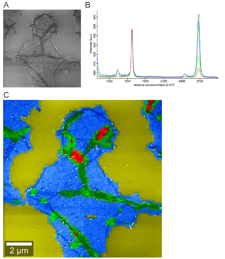
Fig. 1 — RISE microscopy of graphene. (A) SEM image of a graphene sample. (B) Raman spectra of graphene. (C) SEM
image overlaid with the color-coded confocal Raman image. The colors display the graphene layers and wrinkles. Image
parameters: 20 x 20 µm², 150 x 150 pixels = 22,500 spectra, integration time: 0.05 s/spectrum, 1 layer (blue, dark
green), more than 1 layer (light green, red), Si (yellow).
RISE Microscopy of MoS₂
RISE microscopy reveals the structure as well as the crystalline and exciton dynamics of few-layered transition metal
dichalcogenides (TMDs).
CVD-grown monolayers of MoS₂ form triangular two-dimensional crystals. Twin crystals of MoS₂ on SiO₂/Si appear in the
SEM image as star-shaped forms (Figure 2B). The Raman spectra of MoS₂ monolayers show the characteristic E'/E₂g
and A'₁/A₁g Raman band modes of MoS₂ at 385 and 403 relative wavenumbers (cm⁻¹), respectively (Figure 2A). With an
increasing number of layers the two Raman bands drift apart due to in-plane and out-of-plane (inter-layer) vibrations.
Here the green spectrum indicates monolayer MoS₂ while the blue and red spectra signify edges and defects,
respectively.
The spectral information was used to create a Raman image which was overlaid on the SEM image to result in a RISE
image (Figure 2C). The grain boundaries visible in the SEM image correlate perfectly with the areas where Raman
signals indicate wrinkled or overlapping edges, highlighting the effectiveness of RISE imaging for characterizing MoS₂
crystals.
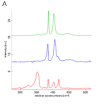
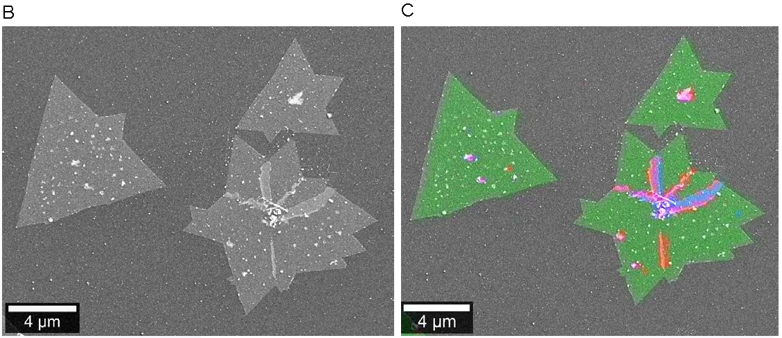
Fig. 2 — RISE microscopy of MoS₂ crystals. (A) Raman spectra of MoS₂: green = 1L MoS₂, blue and red = edges and
defects. (B) SEM image of MoS₂ crystals. (C) Color-coded Raman image derived from the spectral information overlaid
on the SEM image to produce the RISE image. Sample courtesy of Ting Yu, Nanyang Technological University,
Singapore.
Correlative Imaging Reveals Layers and Defects of WS₂ Crystals
WS₂ crystals CVD-grown on a Si/SiO₂ substrate form triangular islands. Atomic Force Microscopy (AFM) was used to
measure their layer thickness (Figure 3A). The flakes are comprised of 1, 2 and more layers. The Raman spectrum of WS₂
displays a typical in-plane (E'/Eg) mode at 352 relative wavenumbers (cm⁻¹) and an out-of-plane (A'₁/A₁g) mode
at 416 relative wavenumbers (cm⁻¹) [1]. The Raman image of the intensity at 416 relative wavenumbers (cm⁻¹) shows that
this signal is strongest in those parts of the crystals that consist of two or more layers and defects, respectively
(Figure 3B).
The number of layers and the type of layer stacking influences not only Raman peaks' intensities and positions
but also the intensity of photoluminescence peaks and their positions. Due to its direct bandgap, monolayer WS₂ shows
a strong PL signal around 635 nm when excited with a 532 nm laser (Figure 3C). This PL signal decreases significantly
with increasing layer numbers because the direct bandgap that is present solely in single-layered TMDs allows for
direct recombination of electrons and holes (Figure 3D). Also the PL peak position varies and PL lifetime changes with
thickness: the more layers the more PL shifts to the red (Figure 3E) and PL lifetime grows shorter (Figure 3F).
Scanning Near-field Optical Microscopy (SNOM) with down to 60 nm spatial resolution was also used for TMD
characterization [2,3]. Here, a strong PL signal indicates edge defects in the material, as shown in a high-resolution
SNOM image of another WS₂ crystal (Figure 3G). These can also be deduced from PL peak position changes (Figure 3H).
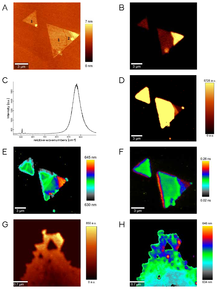
Fig. 3 — Correlative AFM-SNOM-PL imaging of WS₂. (A) AFM image of CVD-grown WS₂ flakes on a Si/SiO₂ substrate
with varying numbers of layers (1, 2, >2). (B) Peak intensity map of the 416 cm⁻¹ Raman mode. (C) PL spectrum
showing strong signal around 635 nm upon 532 nm excitation. (D) PL intensity map at 635 nm corresponding to material
thickness. (E) Position map of PL maxima. (F) PL lifetime map. (G) High-resolution SNOM-PL image of a WS₂ flake
revealing edge defects. (H) SNOM-PL peak position image showing edge defects. Sample courtesy of Ting Yu, Nanyang
Technological University, Singapore.
RISE Imaging and In Situ Modification of WS₂
Here we present the analysis and RISE microscopy imaging of a multi-layered WS₂ crystal. It shows the typical
triangular shape of the material, as well as the heterogeneity of the surface.
A strong WS₂ Raman signal was recorded at approximately 350 relative wavenumbers (cm⁻¹) [4]. Researchers were able to
divide this peak into three sub-peaks [1]. They associated a signal at 344 relative wavenumbers (cm⁻¹) with the
in-plane E' Raman mode. Using this spectral band we generated a Raman intensity map. Overlaying it with the SEM
data produced a RISE microscopy image (Figure 4B).
The Raman signals show that this flake is not homogenously layered. It contains 1L layers and areas with more layers
and also defects. The Raman image corresponds very well to the structures revealed by SEM.
Figure 4C shows the overlay of the SEM image and an intensity peak map of PL. The WS₂ crystal displays strong and
homogenous PL at about 640 nm only in the 1L areas due to the direct bandgap in monolayer WS₂. Defects seen in the SEM
image exhibit PL intensity variations rich in detail. PL intensity corresponds to the intensity of the Raman signal.
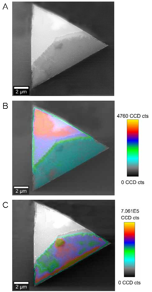
Fig. 4 — Correlative RISE and SEM-PL microscopy of WS₂ crystals. (A) SEM image of a WS₂ flake revealing defects
on the surface and probably adsorbed molecules. (B) The correlative RISE microscopy image composed of the SEM image
and the corresponding Raman intensity map over the 344 cm⁻¹ Raman band, identifying 1L (cyan), 2L (blue) and 3L
(red) areas. (C) Overlay of the SEM and PL intensity images showing that the 3L area lacks PL. Excitation wavelength
for Raman and PL imaging = 532 nm. Sample courtesy of Ting Yu, Nanyang Technological University, Singapore.
Low-Frequency Raman Modes and Imaging of MoSe₂
Not every transition metal dichalcogenide (TMD) can be adequately characterized by its vibrational modes between 200
and 500 relative wavenumbers. In some materials typical in-plane (E'/E₂g) and out-of-plane (A'/A'₁g)
modes, though changing in intensity with increasing thickness of the material, do not show peak shifts. Also, these
primary Raman peaks are highly sensitive to strain and folding [5] and therefore cannot be used to unambiguously
determine the number of layers.
However, low-frequency in-plane shear modes (SM) and out-of-plane layer-breathing modes (LBM) are much more
informative [6]. To measure Raman spectra close to the laser's excitation wavelength at low wavenumbers between 10
and 50 cm⁻¹, efficient blocking of the Rayleigh line while still transmitting adjacent light is necessary. WITec has
developed the RayShield coupler with exactly these features that can be combined with every WITec Raman microscope and
is available for 488, 532, 633 and 785 nm lasers.
All measurements of Figure 5 were carried out by Maria O'Brien, Nigel McEvoy and colleagues (Trinity College,
Dublin). The low-frequency spectrum shows that 1L MoSe₂ has no Raman peak in this range (Figure 5A). With increasing
layer numbers SM and LBM peaks occur, shifting in positions and intensities. Accordingly, the flakes that appear to be
the thinnest in the optical image (Figure 5B) are almost invisible in the Raman image, whereas thicker material can be
detected by their Raman modes (Figure 5C).
The type of layer stacking also influences the Raman peaks' intensities and positions. In stable, semiconducting
MoSe₂ with trigonal prismatic coordination the individual layers can combine in two arrangements, called H and R
stacking. These so-called polytypes cannot be distinguished from each other in optical images but can be by their
distinctive Raman peaks. Intensity changes in Raman modes at 19 and 24 relative wavenumbers (cm⁻¹) reflect differences
in the layer stacking. 2L MoSe₂ displays a typical Raman signal at 19 relative wavenumbers (cm⁻¹) that is more intense
in the 2H than in the 3R stacking configuration (Figure 5D).
From the peak maximum map at 24 relative wavenumbers (cm⁻¹) it is clear that 3L MoSe₂ shows the highest intensity in
the 3R3R configuration followed by 2H3R and inverted 3R3R stacking (Figure 5E). O'Brien and colleagues concluded
that "... low-frequency Raman mapping can distinguish between different stacking configurations rapidly and
non-destructively, allowing TMDs in different stacking configurations to be identified and studied without the need
for high-resolution imaging."
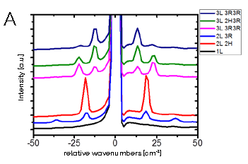
Fig. 5 — Low-frequency Raman modes of MoSe₂. (A) Low-frequency Raman spectra of 1L, 2L and 3L MoSe₂ with various
layer configurations (H and R). (B) Optical image of CVD-grown MoSe₂ revealing differences in thickness and
structure. (C) Map of position of maximum peak intensity over the range of 10 to 40 relative wavenumbers (cm⁻¹). (D)
Peak intensity map of 2L MoSe₂ at 19 relative wavenumbers (cm⁻¹). (E) Peak intensity map of 3L MoSe₂ at 24 relative
wavenumbers (cm⁻¹). Images courtesy of O'Brien, McEvoy and colleagues, Trinity College, Dublin, Ireland.
References
- Peimyoo N., et al. (2013). Nonblinking, intense two-dimensional light emitter: monolayer WS2 triangles. ACS
nano
- , 7(12), 10985–10994.
- Lee, Y., et al. (2015). Characterization of the structural defects in CVD-grown monolayered MoS2 using near-field
photoluminescence imaging. Nanoscale
- , 7(28), 11909–11914.
- Lee, Y., et al. (2017). Near-field spectral mapping of individual exciton complexes of monolayer WS2 correlated
with local defects and charge population. Nanoscale
- , 9(6), 2272–2278.
- Wang, Y., et al. (2015). Strain-induced direct–indirect bandgap transition and phonon modulation in monolayer WS2.
Nano Research
- , 8, 2562–2572.
- Zhang, X., et al. (2013). Raman spectroscopy of shear and layer breathing modes in multilayer MoS2. Physical
Review B — Condensed Matter and Materials Physics
- , 87(11), 115413.
- O'Brien, M., et al. (2016). Mapping of low-frequency Raman modes in CVD-grown transition metal
dichalcogenides: Layer number, stacking orientation and resonant effects. Scientific reports
- , 6(1), 19476.

