Analyzing Solar Cell Material Properties with Confocal Raman Imaging
Energy generation using photovoltaic devices is regarded as an important component in overcoming future energy shortages. This is reflected in a dramatic increase in photovoltaic production and demand. In the research and development of photovoltaic devices, the primary goals are to increase the conversion efficiency of the solar cells or to improve the production process. For these studies, a detailed knowledge of the micro- and nanostructures along with the chemical properties is essential for further improvements. A valuable tool for these investigations is Confocal Raman Imaging, as it not only reveals optical information but also information regarding the 3D distribution of the chemical compounds, crystallinity and material stress. The Fraunhofer-Institute for Solar Energy Systems (ISE), one of the leading institutes in the research and development of solar cell systems, employs the alpha500 Confocal Raman AFM Microscope for the analysis of photovoltaic (PV) cells and polymeric module components. In a joint research project, WITec and the ISE (Durability Analysis and Environmental Engineering Group) investigated several solar cell samples relevant to the solar cell industry using Confocal Raman Microscopy. This article describes the application of Confocal Raman Imaging for the analysis of stress fields around laser-drilled holes on a Si solar cell as well as the investigation of concentration-dependent properties of a dye solar cell.
Stress Fields Surrounding a Laser-drilled Hole on a Si Solar Cell Device
Typical Si-based solar cells are principally built as shown in Fig. 1 (sample courtesy of Fraunhofer-Institute for Solar Energy Systems ISE). The contacts for discharging are located on top of the p- and n-doped material. It is now generally considered better to avoid placing the contacts on the top surface, as they block some of the sunlight and thus lower the efficiency. Therefore holes need to be drilled through the solar cells in order to allow the contacts to be located on the bottom of the solar cells. These holes are typically drilled with lasers. The drilling process however can induce strain in the Si around the holes, which in turn lowers the efficiency of the solar cells. In this study two ways of minimizing the stress are investigated:
- Minimizing the laser power for drilling using:
- a) 100% drilling power with 9 repetitions
- b) 20% drilling power with 20 repetitions
- Etching the wafer after the drilling process:
- a) no etching
- b) 1 Minute etching with KOH
- c) 2 Minutes etching with KOH
- d) 4 Minutes etching with KOH
- e) 6 Minutes etching with KOH
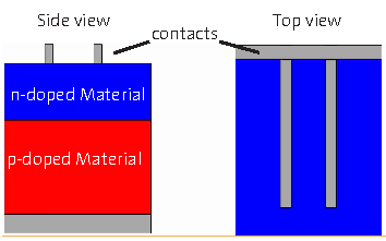
Fig. 1 — Typical set-up of a solar cell.
In order to evaluate the strain induced by the drilling on the Si around the holes, Confocal Raman Imaging was used. These measurements were performed with a WITec alpha700 system using a 532 nm excitation laser (approximately 17 mW on the sample), a 100x air objective (NA 0.9). The scattered light was directed to the spectrometer using a 50 µm core diameter multimode fiber which also acts as the pinhole for confocal detection. The spectrometer was a WITec UHTS 300 equipped with a back-illuminated CCD camera and 1800 grooves/mm grating. The integration time for each spectrum was 23 ms and 150x150 pixels (=22500 spectra) over an area of 35x35 µm. The total acquisition time per image was less than 10 minutes. Some of the holes showed splashes of Si on the surface of the wafer which resulted in a higher 1st order Si peak on these structures, as shown in Fig. 2, where the integrated intensity of the Si peak is evaluated at each pixel and displayed as an image. However, these areas were avoided for the strain measurements, while holes with relatively smooth looking surroundings (see Fig. 3 for example) were selected.
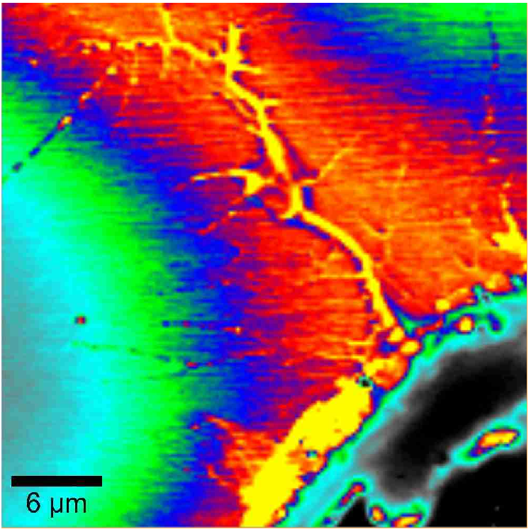
Fig. 2 — Splash of Si onto the surface out of the hole (bottom right). Plotted is the integrated intensity of the 1st order Si peak.
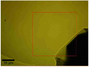
Fig. 3 — Video image of a typical scan area (red box) on the Si. The hole is visible on the bottom right corner.
For each image the 1st order Si peak was fitted using a Lorentzian curve and the exact peak position was then evaluated. This could also be shown as an image and an example is shown in Fig. 4. From these images, cross-sections as shown in Fig. 4 were extracted and plotted as relative peak positions (in rel. 1/cm) vs. distance (note that the starting point relative to the edge of the hole varies for each line). Figures 5 and 6 show the results of these evaluations. Fig. 5 shows the results for the samples with full drilling power and the different etching processes applied to the samples are indicated by the colors [no etching (red), 1 min etching (blue), 2 min etching (green), 4 min etching (black), 6 min etching (magenta)]. Fig. 6 uses the same color coding, but shows the results for the cases drilled with only 20% power. For most graphs a slight decrease in the peak position can be seen starting from the left side of the graph and moving towards the position of the drilled hole. These are presumably long-range stress fields in the Si. Close to the edge of the hole, the stress in the Si increases and changes dramatically and then inside the hole, no proper Si signal could be detected.
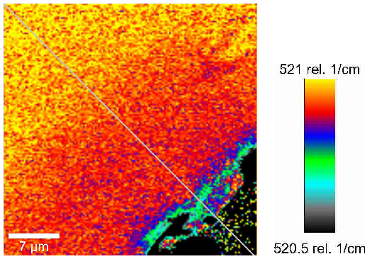
Fig. 4 — A typical stress map of the Si (position of the 1st order Si line) from the outside to the hole (bottom right). Along the indicated cross section (gray line), the radial change of the stress field was evaluated.
From Fig. 5 it can clearly be seen that the sample which had not been etched as well as the sample which had been etched for only 1 minute show a clear drop of the peak position before reaching the edge of the hole. This drop is eliminated for the other cases. From Fig. 6 the same conclusion as above can be drawn. Additionally, the graphs seem to indicate that the soft drilling process reduces the far-reaching stress field (the slope of the lines). Both graphs indicate that an etching process of 2 minutes is sufficient.
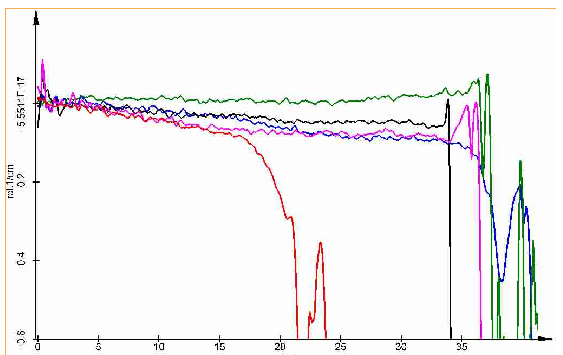
Fig. 5 — The cross sections of the various samples drilled with 100% laser power: no etching (red), 1 min etching (blue), 2 min etching (green), 4 min etching (black), 6 min etching (magenta).
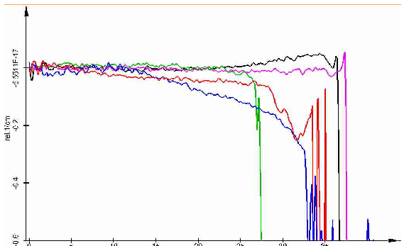
Fig. 6 — The cross sections of the various samples drilled with 20% laser power: no etching (red), 1 min etching (blue), 2 min etching (green), 4 min etching (black), 6 min etching (magenta).
Dye Solar Cells
A test array for the observation of the distribution of the dye (attached to the TiO2) and the evaluation of the iodide in dye base solar cells was prepared as shown in Fig. 7 (sample courtesy of Fraunhofer-Institute for Solar Energy Systems ISE). The iodide concentration varied in the samples from 0% to 600% of the concentration typically used in dye bases solar cells.
The investigated cells had the following structure:
- Glass with TCO (Transparent Conductive Oxide, 3 mm total thickness)
- Inner area (total thickness ca. 30–35 µm):
- TiO2 nano-porous area (ca. 10 µm)
- Monolayer dye
- Electrolyte consisting of:
- ACN (acetonitril)
- Ionic liquid (contains single iodide ions)
- Iodide (varying in concentration and forming tri-iodide-ions)
- Pt-layer as the catalyst
In the transparent areas of the cells (see Fig. 7) no TiO2 was applied and therefore no dye was present.
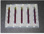
Fig. 7 — Image of the dye solar cell samples. The concentration of the iodine changes from left to right as 600%, 200%, 100%, 50%, 0%. In the clear parts on top of the cells no dye was present.
As a first step, single spectra (10 accumulations with 2 s integration time) were taken from the areas without dye (through the 3 mm glass) in order to evaluate the change in the spectra subjected to the iodide concentration changes (Fig. 8). It can clearly be seen that the peak associated with iodide (located near 110 rel. 1/cm) is rising with the iodide concentration. However, at 0% there is still a significant peak present. This is due to the ionic liquid which itself contains iodide ions.
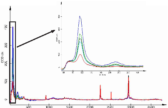
Fig. 8 — The change in the spectra as a function of the iodine concentration: red = 0%; turquoise = 50%; black = 100%; green = 200%; blue = 600%.
In a second step, the border area between the dye-containing area and the transparent area was imaged (again through the 3 mm glass). The image was acquired using a 50x objective (NA 0.5) with 80x80 pixels (=6400 spectra) and a scan range of 50x50 µm. For excitation, a 532 nm NdYag laser was used. Acquisition time for one spectrum was 213 ms. The resulting spectra are shown in Fig. 9 and also a zoomed view of the finger-print area in Fig. 10.
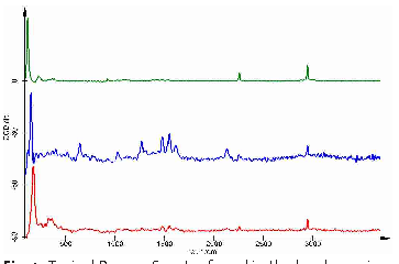
Fig. 9 — Typical Raman spectra found in the border region of the dye solar cell.
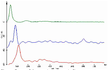
Fig. 10 — Zoom of the spectra as seen in Fig. 9.
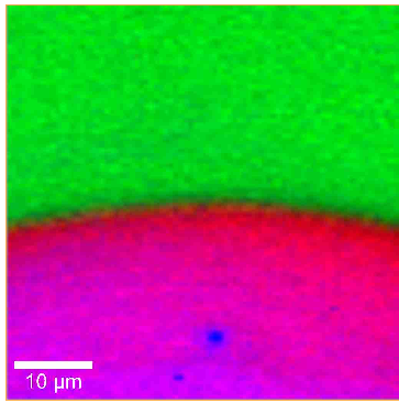
Fig. 11 shows the corresponding confocal Raman image with the colors indicating where each spectrum can primarily be found. Note that violet areas indicate that a mixture of the blue and red spectra can be found at these areas. The image in combination with the spectra indicate that the ionic liquid plus the ACN (green spectrum) can be found in the green area. The area filled as in standard dye solar cells (darker areas in Fig. 7 and violet area in Fig. 11) shows a significantly lower signal for the green spectrum but a strong signal of a mixture of the red and blue spectra. The blue spectrum shows the characteristic peaks of the dye near 1500 rel. 1/cm, the intense peak near 155 rel. 1/cm and characteristic peak at about 165 rel. 1/cm. It is interesting that this additional spectrum and thus also the material from which this originates seems to be present without the dye at the transition area between the green and the violet area.

